Input device
A technology of an input device and a detection layer, which is applied to the field of input devices in which electrostatic capacitance type detection parts are overlapped, can solve the problems of reduced detection accuracy of the pressure-sensitive detection part, difficulty in thinning, and increased cost, etc. The effect of lower assembly cost, lower material cost, easy work
- Summary
- Abstract
- Description
- Claims
- Application Information
AI Technical Summary
Problems solved by technology
Method used
Image
Examples
Embodiment Construction
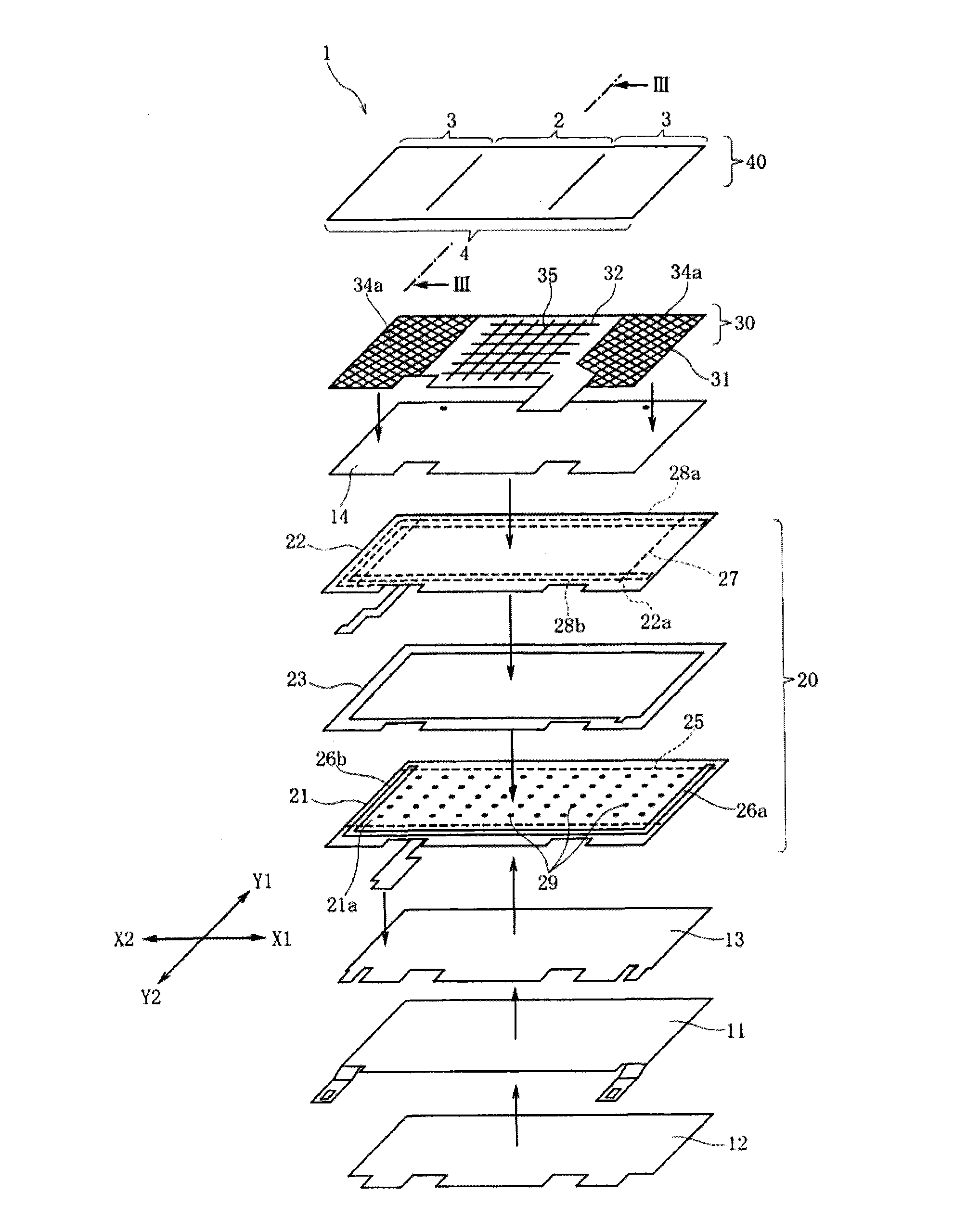
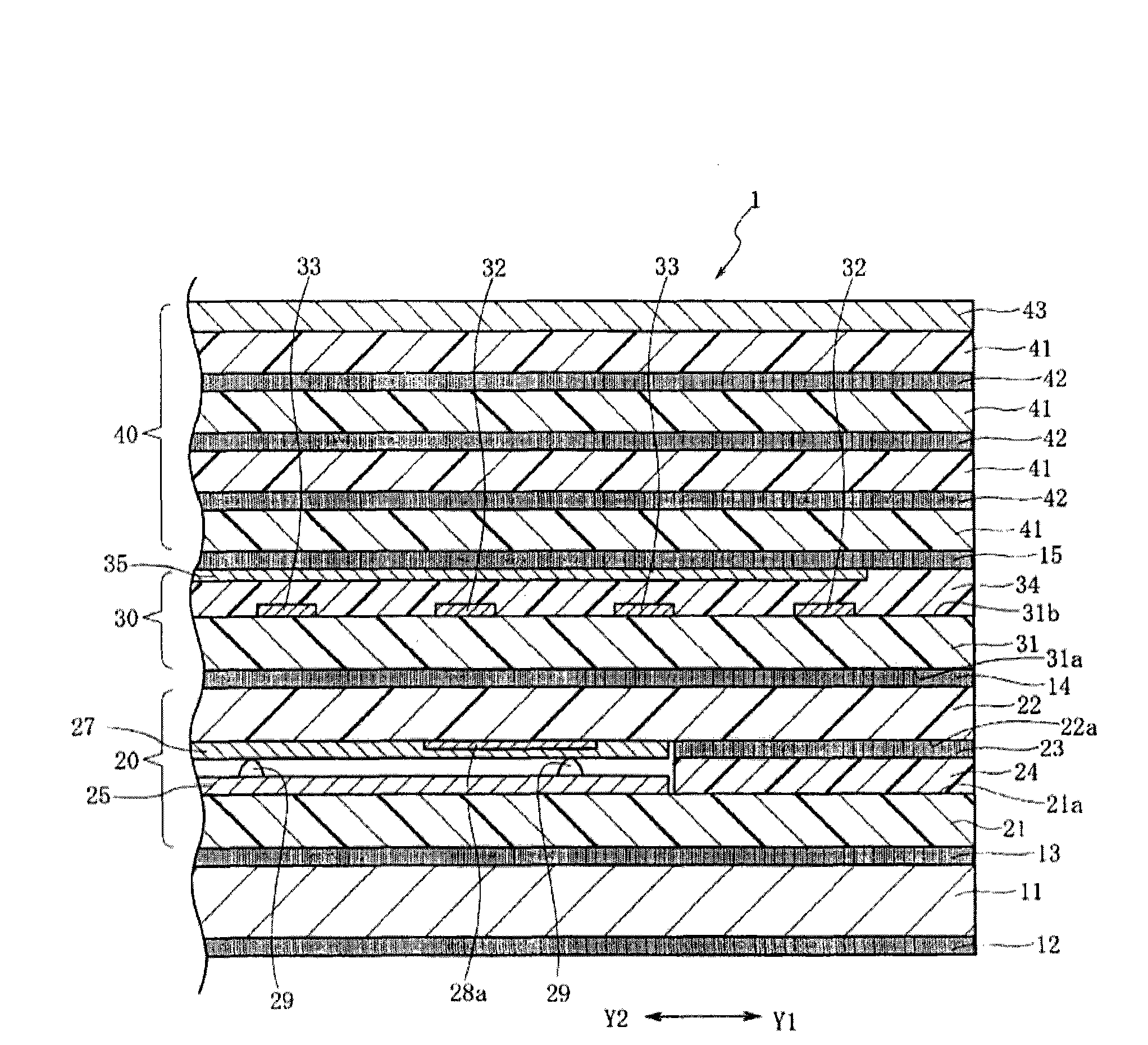
[0033] figure 1 It is an exploded perspective view showing the input device according to the first embodiment of the present invention, figure 2 It is an exploded perspective view showing the structure of a capacitive detection unit included in the above-mentioned input device, image 3 for from figure 1 An enlarged partial cross-sectional view of the cross-sectional view of the input device according to the first embodiment viewed from the direction indicated by the arrow III.
[0034] Such as figure 1 and figure 2 As shown, the input device 1 of the first embodiment has a rectangular shape in which the long side faces the X direction and the short side faces the Y direction. The central part of the input device 1 in the X direction is an electrostatic detection area 2 , and the two sides thereof are extension parts 3 , 3 . Almost the entire area including the electrostatic detection area 2 and the extensions 3 , 3 is a pressure-sensitive detection area 4 . image 3 T...
PUM
 Abstract
Description
Claims
Application Information
 - R&D
- Intellectual Property
- Life Sciences
- Materials
- Tech Scout
- Unparalleled Data Quality
- Higher Quality Content
- 60% Fewer Hallucinations
Browse by: Latest US Patents, China's latest patents, Technical Efficacy Thesaurus, Application Domain, Technology Topic, Popular Technical Reports.
© 2025 PatSnap. All rights reserved.Legal|Privacy policy|Modern Slavery Act Transparency Statement|Sitemap|About US| Contact US: help@patsnap.com


