Image sensor and fabrication method thereof

A technology of an image sensor and a manufacturing method, which is applied in the field of image sensors, can solve the problems that optical waveguides are not widely used in sensors, and the complexity and manufacturing cost of image devices are increased.

Inactive Publication Date: 2009-07-29
VISERA TECH CO LTD
View PDF0 Cites 12 Cited by
  • Summary
  • Abstract
  • Description
  • Claims
  • Application Information

AI Technical Summary

Problems solved by technology

However, optical waveguides are not widely used to concentrate light to sensors in imaging devices
In addition, the manufacture of the currently used optical waveguide structure requires additional manufacturing process steps, thus increasing the complexity and manufacturing cost of the image device.

Method used


Image

  • Image sensor and fabrication method thereof
  • Image sensor and fabrication method thereof
  • Image sensor and fabrication method thereof

Examples


Embodiment Construction

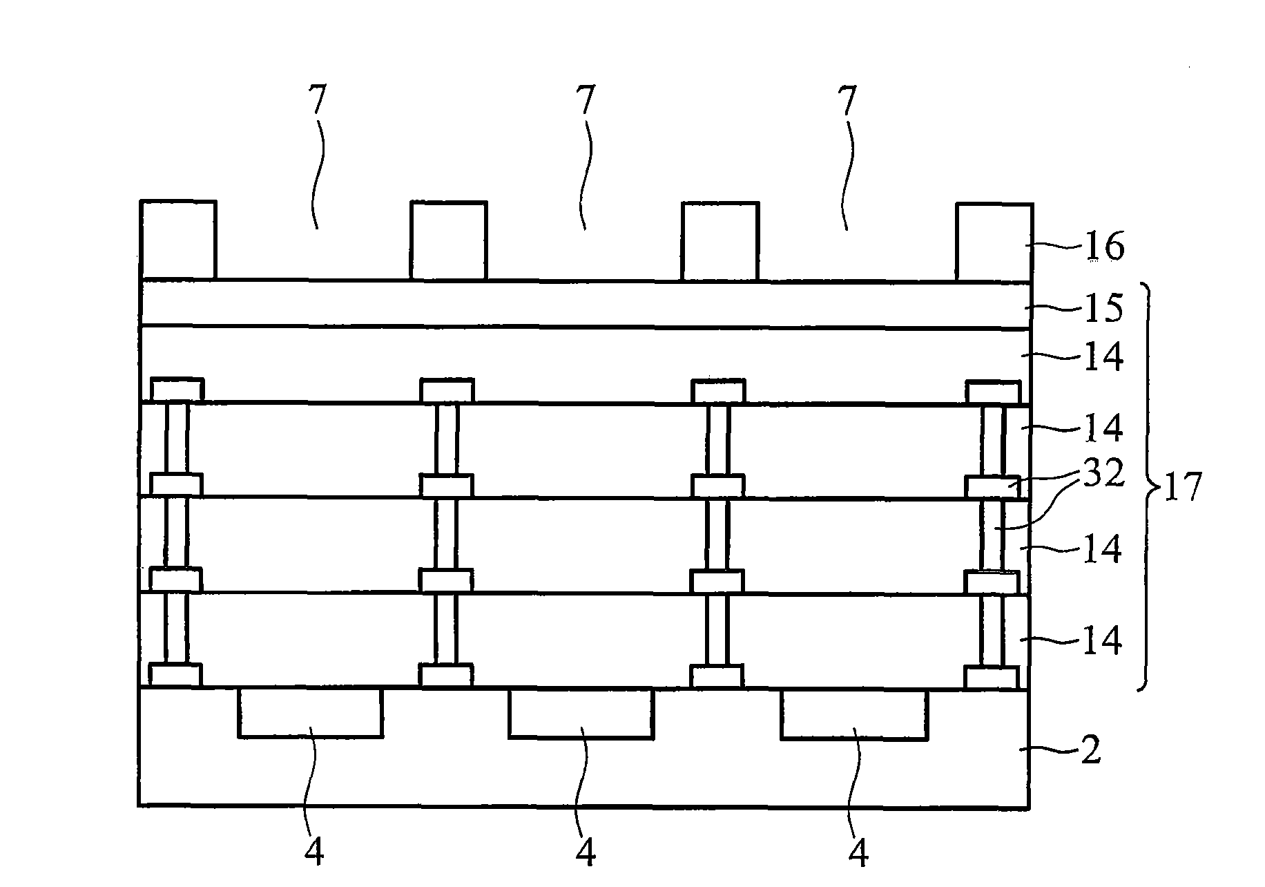
[0026] Embodiments of the present invention provide a method for manufacturing a photo-sensing integrated circuit and an image sensor. The manufacturing and usage methods of each embodiment are described in detail below and illustrated with accompanying drawings. Wherein, the same reference numerals used in the drawings and the specification represent the same or similar components. In the accompanying drawings, for the sake of clarity and convenience of illustration, the shapes and thicknesses of the embodiments may be unrealistic. The following description is specifically directed to the various elements of the device of the present invention or their integration. However, it is worth noting that the above-mentioned elements are not particularly limited to what is shown or described herein, but can be familiar with the ordinary technology in this technical field. In addition, when a material layer is on top of another material layer or substrate, it may be directly on its su...


PUM


Abstract

The present invention provides an image sensor and method for producing the same, wherein the image sensor comprises a substrate comprising a plurality of optical sensor units located therein or thereon; a plurality of optical guide structures corresponding to the plurality of optical sensor units respectively; and a stacked layer surrounding the optical guide structures, comprising a plurality of top portions with sharp corners adjacent to the top edges of the optical guide structures. The invention can not only prevent possible cross talk disturbance caused by stray light shooting into adjacent groove hence improve sensitivity of optical sensor units.

Description

technical field [0001] The invention relates to an image sensor, and in particular to a manufacturing method of a color image sensor. Background technique [0002] Many digital imaging devices (such as digital cameras) require image sensors, such as charge-coupled devices (CCDs) and complementary metal-oxide-semiconductor (CMOS) image sensors. An image sensor includes a two-dimensional array of photosensitive array devices (eg, photosensitive cells) that convert images into electronic signals. The display, in turn, receives signals from the photosensitive device of the image sensor and forms a representative image. [0003] Light sensitivity is very important for an image sensor because the photosensitive device can store signals to reflect the intensity or brightness of light associated with an image. [0004] However, reflection or refraction of light radiation in image sensing pixels is often the main cause of cross-talk in image sensors. If the reflection or refractio...

Claims


Application Information

Patent Timeline
Patent Type & Authority Applications(China)
IPC IPC(8): H01L27/146H01L21/84H01L21/82
CPCH01L27/14621H01L27/14685H01L27/14627H01L27/14629
Inventor 林建邦许中荣颜秀芳刘宇杰
Owner VISERA TECH CO LTD
Why Eureka
Try Eureka