


Quick Research
Generate reliable direction feasibility study reports for your R&D in just a few steps.

Technical Q&A
Discover and master advanced knowledge NOW. Basics, ideas, possibilities, all at once.

Find Solutions
As an expert in R&D theories, this can generate solutions to your technical problems instantly.

Evaluate Feasibility
Analyze your overall solution with one click, know your potential R&D risks in advance.

Monitor Landscape
Get weekly tech updates, stay abreast of the latest tech innovations and key insights.
Semiconductor device with test structure and semiconductor device test method
A technology for testing structures and semiconductors, applied in the directions of instruments, measuring electricity, measuring devices, etc., can solve the problems of inability to detect transistors, etc., and achieve the effect of easy structural change and easy determination
- Summary
- Abstract
- Description
- Claims
- Application Information
AI Technical Summary
Problems solved by technology
Method used
Image

Examples
Embodiment Construction
[0026] It should be understood that the drawings are only schematic and not drawn to scale. It should also be understood that the same reference numerals are used throughout the drawings to designate the same or similar parts.
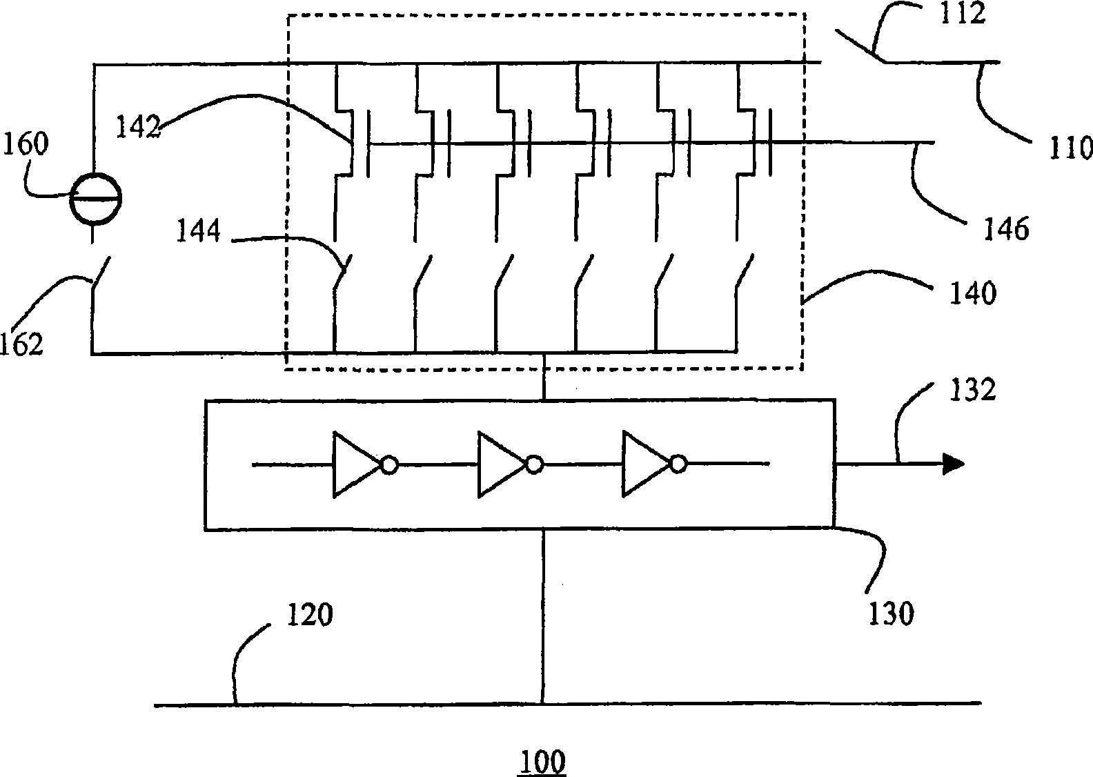
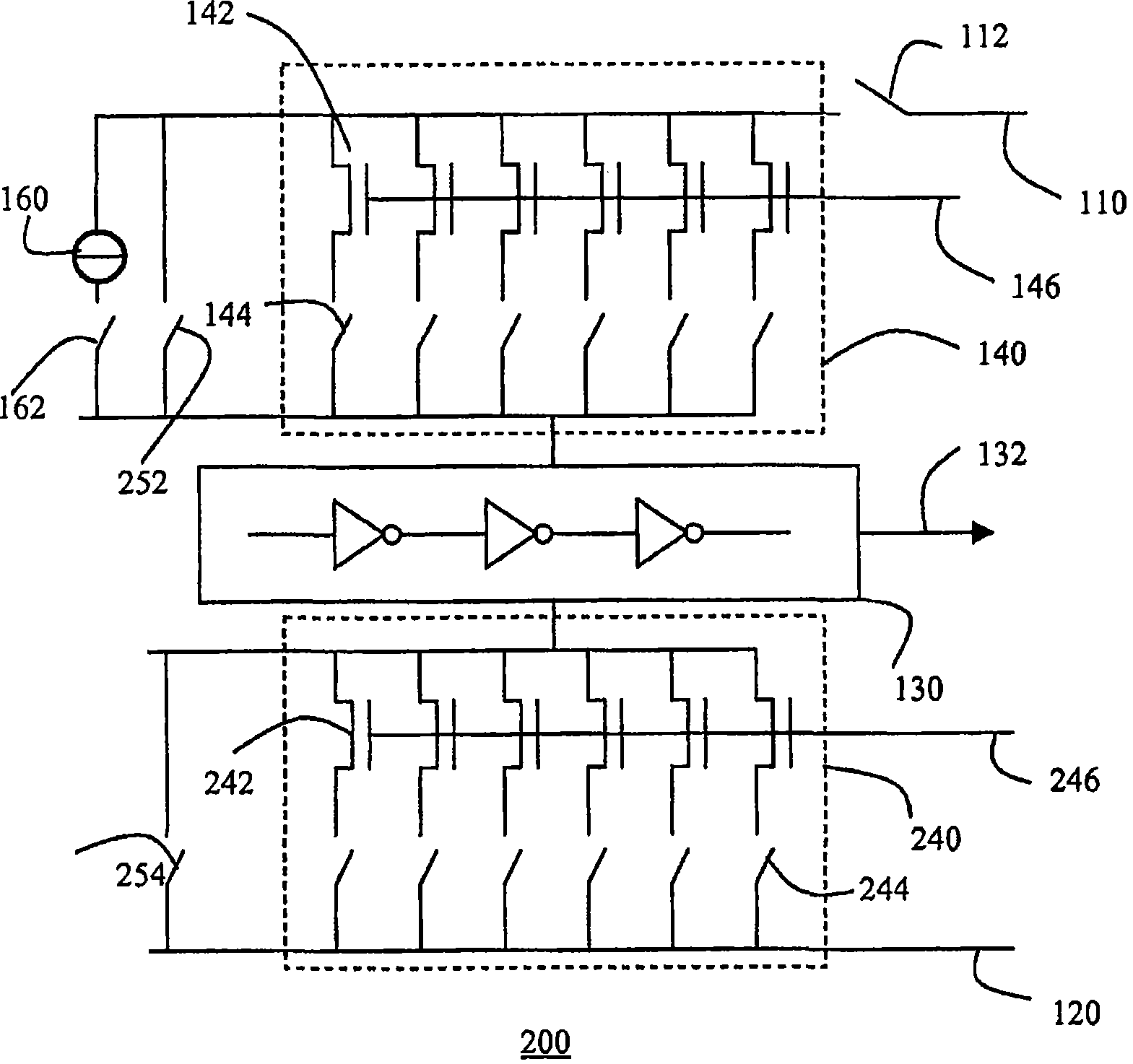
[0027] exist figure 1 1 , a semiconductor device (which may be an IC or a wafer carrying multiple ICs) has a test structure 100 including a ring oscillator 130 coupled between a first supply rail 110 and a second supply rail 120 . The ring oscillator 130 has an output 132 at which the output frequency of the ring oscillator 130 is provided. Output 130 may be coupled to an output pin (not shown) of a semiconductor device. The conductive coupling between the first power rail 110 and the ring oscillator 130 includes an array 140 of transistors 142 . Transistor 142 may be implemented using any suitable technology, such as without limitation CMOS technology. Furthermore, transistors 142 do not have to be the same size. This will depend on the specific ...
PUM
 Abstract
Description
Claims
Application Information
 - R&D Engineer
- R&D Manager
- IP Professional
- Industry Leading Data Capabilities
- Powerful AI technology
- Patent DNA Extraction
Browse by: Latest US Patents, China's latest patents, Technical Efficacy Thesaurus, Application Domain, Technology Topic, Popular Technical Reports.
© 2024 PatSnap. All rights reserved.Legal|Privacy policy|Modern Slavery Act Transparency Statement|Sitemap|About US| Contact US: help@patsnap.com