Semiconductor device and its manufacturing method
A manufacturing method and semiconductor technology, applied in semiconductor/solid-state device manufacturing, semiconductor devices, electrical components, etc., can solve the problems of insufficient cost and expensive manufacturing, and achieve the effect of high withstand voltage and low on-resistance
- Summary
- Abstract
- Description
- Claims
- Application Information
AI Technical Summary
Problems solved by technology
Method used
Image
Examples
no. 1 approach
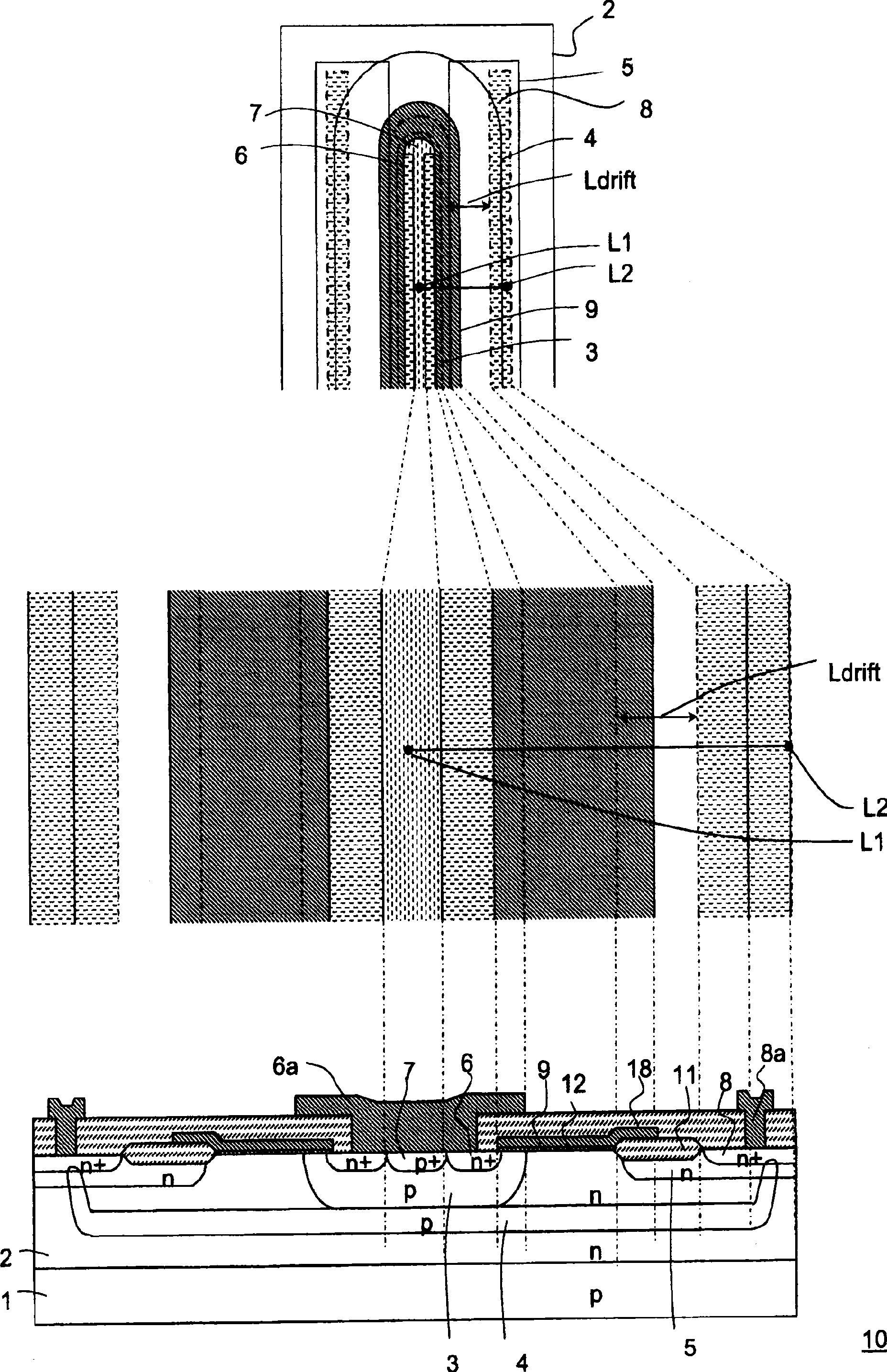
[0077] will refer to Figure 1-8 The device and method of the present invention according to the first embodiment mode (hereinafter occasionally referred to as "the present embodiment mode") are described.
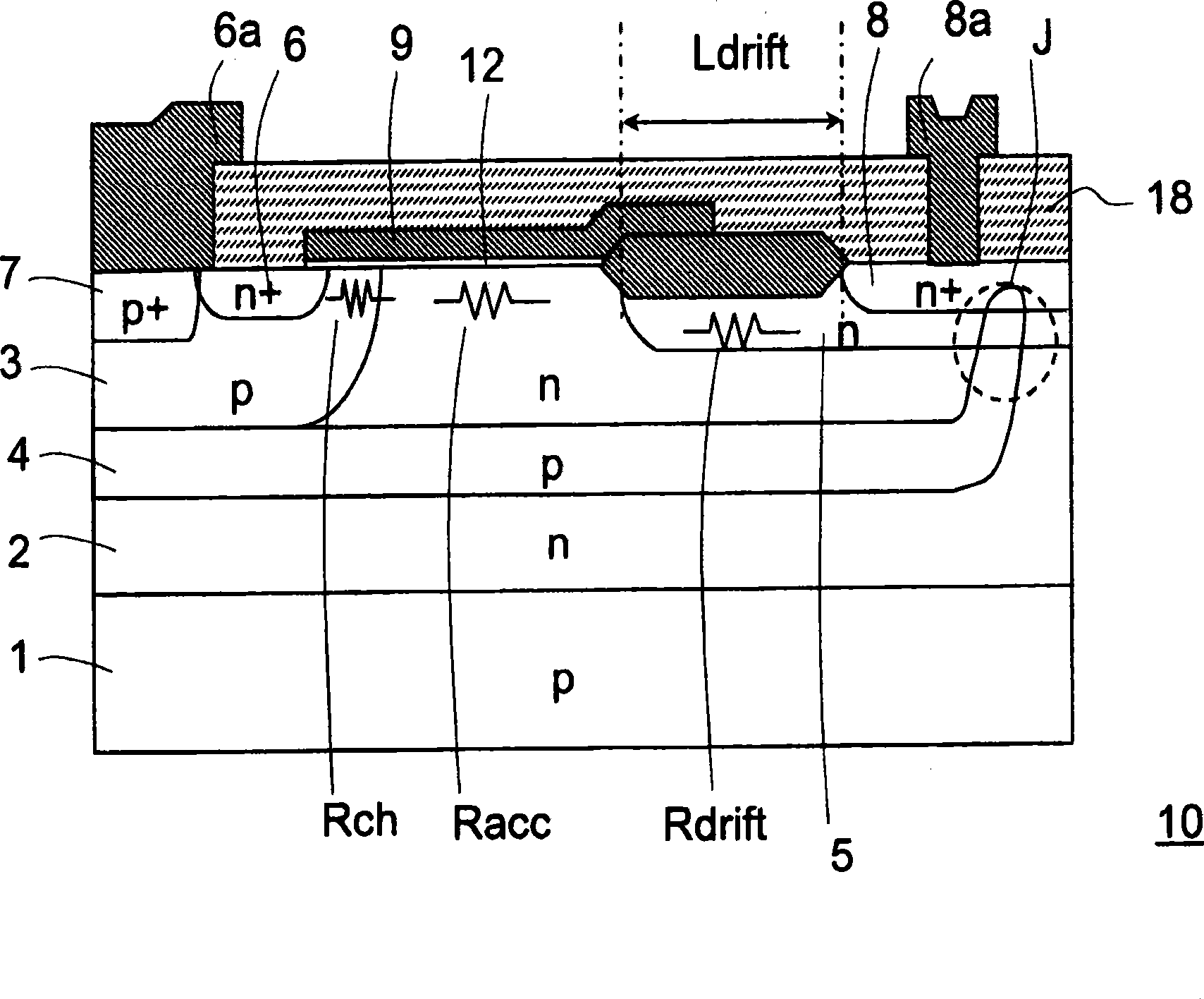
[0078] figure 1 is a schematic plan view showing a semiconductor device of the present invention according to this embodiment mode. also, figure 2 is showing figure 1 An enlarged view and a schematic cross-sectional view of a part of a device of the present invention are shown. Here, the cross-sectional view schematically shows the structure, and the dimensions in the drawings do not necessarily match the actual ones. The same is true in the following embodiments. Additionally, with Figure 19 to Figure 2 Components that are the same as those in 2 are denoted by the same symbols throughout the drawings.
[0079] exist figure 1 and 2 The device 10 of the present invention shown in is composed of P-type semiconductor substrate 1, N-type well region 2, P-type bod...
no. 2 approach
[0103] will refer to Figure 9-1 2 Describe the device and method of the present invention according to the second embodiment (hereinafter referred to as "the present embodiment").
[0104] Figure 9 is a schematic plan view showing a device of the present invention according to this embodiment mode. also, Figure 10 is showing Figure 9 An enlarged view and a schematic cross-sectional view of a part of a device of the present invention are shown. Here, the same components as those in the first embodiment are denoted by the same symbols, so descriptions thereof will not be given here.
[0105] Such as Figure 9 and 10 As shown, the device 10 a of the present invention according to this embodiment differs from the first embodiment in that the body region 3 is formed to surround the drain region 8 . The rest of the configuration is similar to that in the first embodiment.
[0106] The present embodiment has a structure in which the drain region 8 is formed in the central...
no. 3 approach
[0119] will refer to Figure 13 and 14 A device and method of the present invention according to a third embodiment mode (hereinafter referred to as "this embodiment mode") are described.
[0120] Figure 13 are a schematic plan view and a schematic cross-sectional view showing a device of the present invention according to this embodiment mode. Here, the same components as those in the first and second embodiments are denoted by the same symbols, so descriptions thereof will not be given here.
[0121] Such as Figure 13 As shown, the device 10b of the invention according to this embodiment is formed in such a way that the body region 3 surrounds the drain region 8, as in the device 10a of the invention according to the second embodiment. Furthermore, as in the second embodiment, P-type buried diffusion region 4 is formed so as to be in contact with the bottom of body region 3 , and P-type buried diffusion region 4 extends to a region below drain region 8 . Furthermore, ...
PUM
 Abstract
Description
Claims
Application Information
 - R&D Engineer
- R&D Manager
- IP Professional
- Industry Leading Data Capabilities
- Powerful AI technology
- Patent DNA Extraction
Browse by: Latest US Patents, China's latest patents, Technical Efficacy Thesaurus, Application Domain, Technology Topic, Popular Technical Reports.
© 2024 PatSnap. All rights reserved.Legal|Privacy policy|Modern Slavery Act Transparency Statement|Sitemap|About US| Contact US: help@patsnap.com


