Surface emitting laser, surface emitting laser array, and image forming apparatus including surface emitting laser
A surface emission and laser technology, applied in laser devices, semiconductor laser devices, lasers, etc., can solve the problems of difficult preparation of AlAs layers
- Summary
- Abstract
- Description
- Claims
- Application Information
AI Technical Summary
Problems solved by technology
Method used
Image
Examples
no. 1 example
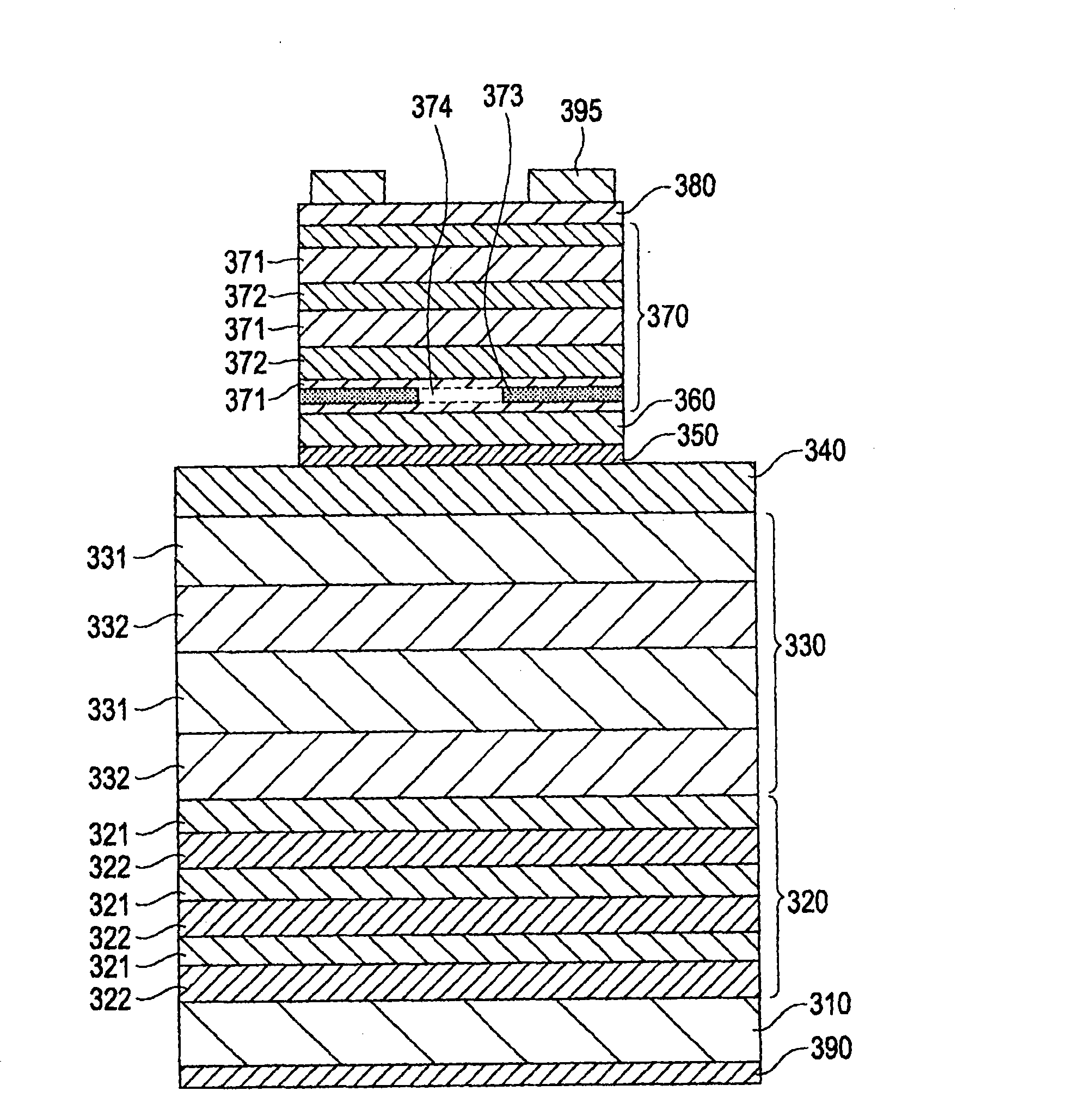
[0056] image 3 is a schematic cross-sectional view of the red surface emitting laser according to the first embodiment.
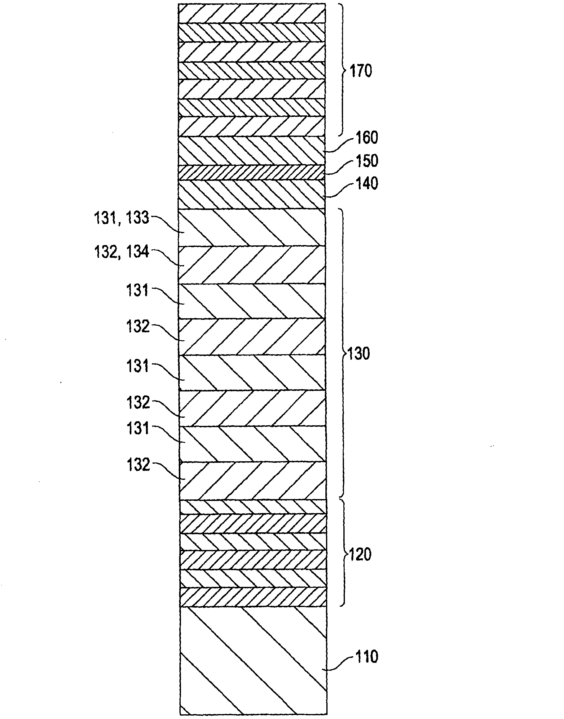
[0057] The lower DBR 320 is disposed on the n-type GaAs substrate 310 . The lower DBR 320 includes alternately stacked n-type AlAs sublayers 321 and n-type Al 0.5 Ga 0.5 As sublayer 322 . n-type AlAs sublayer 321 and n-type Al 0.5 Ga 0.5 Each of the As sublayers 322 has an optical thickness of λ / 4. Although the lower DBR 320 is shown for convenience to contain three pairs of n-type AlAs sublayers 321 and Al 0.5 Ga 0.5 As sublayer 322, but lower DBR 320 may actually contain as many pairs as desired (eg, 60 pairs).
[0058] A spacer layer 330 is disposed on the lower DBR 320 . The spacer layer 330 includes alternately stacked first AlAs semiconductor sub-layers 331 and second Al 0.5 Ga 0.5 As semiconductor sublayer 332 . Each of the first semiconductor sublayer 331 and the second semiconductor sublayer 332 has an optical thickness of λ / 2. As not...
no. 2 example
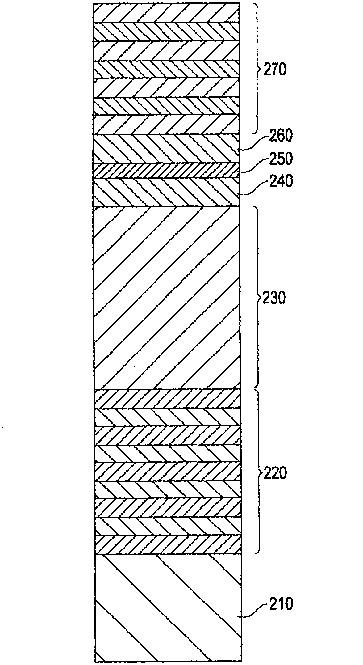
[0089] Figure 5 is a schematic cross-sectional view of a surface emitting laser according to a second embodiment. The same reference numerals used in the second embodiment as in the first embodiment denote the same components.
[0090] The surface-emitting laser according to the second embodiment includes a spacer layer 530 as in the first embodiment. However, the second embodiment differs from the first embodiment in that the sublayers constituting the spacer layer 530 have different thicknesses.
[0091] More specifically, an AlAs sublayer 533 with a thickness of 540 nm is provided directly under the AlGaInP layer 340, and an Al layer with a thickness of 290 nm is provided directly under the AlAs sublayer 533 0.5 Ga 0.5 As layer 534 . Thus, AlAs sublayer 533 has an optical thickness of (5λ) / 2, and Al 0.5 Ga 0.5 The As sublayer 534 has an optical thickness of (3λ) / 2. The AlAs sublayer 533 having an optical thickness greater than λ / 2 can effectively dissipate heat from...
no. 3 example
[0095] Figure 6 is a schematic cross-sectional view of a surface-emitting laser according to a third embodiment. The same reference numerals used in the third embodiment as in the first embodiment denote the same components.
[0096] The third embodiment differs from the first embodiment in that the uppermost sublayer of the spacer layer 630 disposed directly under the AlGaInP layer 340 is Al 0.9 Ga 0.1 As sublayer 601 . Therefore, the first AlAs semiconductor sublayer in the first embodiment is covered by Al 0.9 Ga 0.1 As sublayer 601 instead.
[0097]This structure is adopted for the following reason: the uppermost AlAs sublayer of the spacer layer exposed when the mesa structure is formed by dry etching is oxidized during the formation of the current confinement structure. Therefore, the structure according to the third embodiment can increase the yield of laser devices. instead of Al 0.9 Ga 0.1 As, AlGaAs having an Al / (Al+Ga) atomic ratio of 0.95 or less or 0.90 ...
PUM
 Abstract
Description
Claims
Application Information
 - R&D
- Intellectual Property
- Life Sciences
- Materials
- Tech Scout
- Unparalleled Data Quality
- Higher Quality Content
- 60% Fewer Hallucinations
Browse by: Latest US Patents, China's latest patents, Technical Efficacy Thesaurus, Application Domain, Technology Topic, Popular Technical Reports.
© 2025 PatSnap. All rights reserved.Legal|Privacy policy|Modern Slavery Act Transparency Statement|Sitemap|About US| Contact US: help@patsnap.com


