Transistor resistance and correlation method
A transistor resistance, transistor technology, applied in the direction of resistors, circuits, diodes, etc., can solve problems such as poor linearity and resistance value changes
- Summary
- Abstract
- Description
- Claims
- Application Information
AI Technical Summary
Problems solved by technology
Method used
Image

Examples
Embodiment Construction
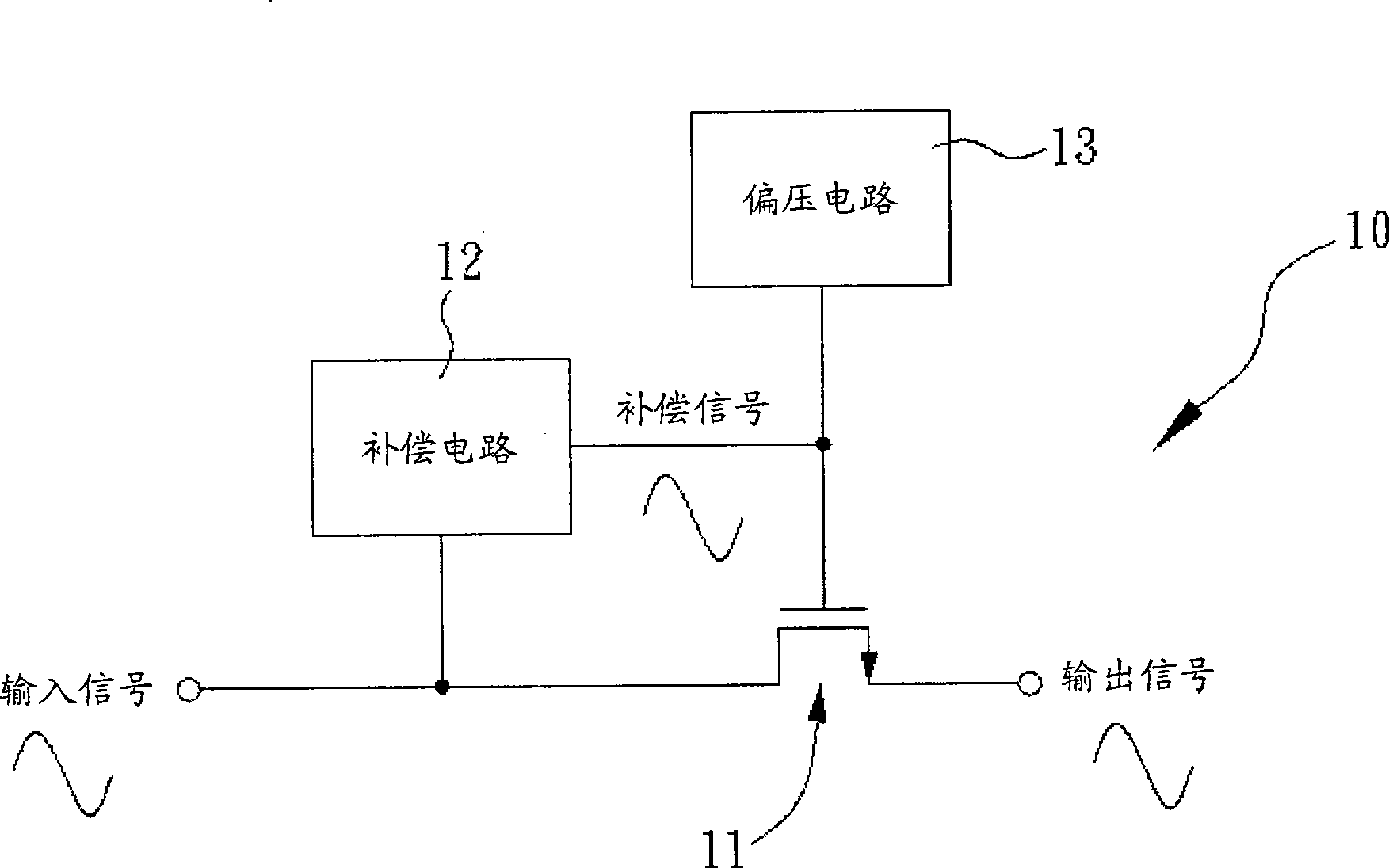
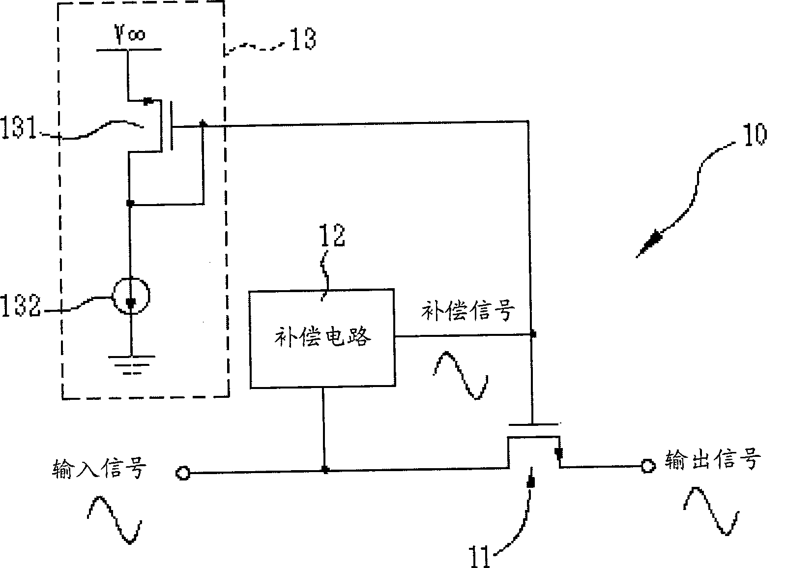
[0022] This description takes a MOS transistor as an example, but it is not limited thereto. Figure 1A is a schematic diagram of an embodiment of the transistor resistor of the present invention. In the figure, the transistor resistor 10 includes an NMOS transistor 11 , a compensation circuit 12 and a bias circuit 13 . The NMOS transistor 11 operates in the resistive region, that is, its gate-to-source voltage v GS Need to be greater than the threshold voltage (threshold vol tage) V T , and the drain-to-source voltage v DS need to be small. When the NMOS transistor 11 operates in the resistance region, there will be a current i D flows into its drain and out of its source, and i D with v DS The relationship between
[0023] i D =2K(v GS -V T )v DS Formula 1)
[0024] in, K = 1 2 μ n C ox W L ...
PUM
 Abstract
Description
Claims
Application Information
 - R&D
- Intellectual Property
- Life Sciences
- Materials
- Tech Scout
- Unparalleled Data Quality
- Higher Quality Content
- 60% Fewer Hallucinations
Browse by: Latest US Patents, China's latest patents, Technical Efficacy Thesaurus, Application Domain, Technology Topic, Popular Technical Reports.
© 2025 PatSnap. All rights reserved.Legal|Privacy policy|Modern Slavery Act Transparency Statement|Sitemap|About US| Contact US: help@patsnap.com