Method for making flash memory

A memory and flash technology, applied in the field of making flash memory, can solve problems such as memory defect operation life, save process cost and avoid read and write failures

Active Publication Date: 2010-06-02
POWERCHIP SEMICON MFG CORP
View PDF4 Cites 0 Cited by
  • Summary
  • Abstract
  • Description
  • Claims
  • Application Information

AI Technical Summary

Problems solved by technology

[0006] The method of the present invention is to provide a method for manufacturing a flash memory, which is a method for improving the cross-sectional shape of a floating gate by using a grinding buffer layer and a grinding process, so as to solve the above-mentioned problem of forming active region trenches in an etching process. Causes problems such as memory defects and short operating life

Method used


Image

  • Method for making flash memory
  • Method for making flash memory
  • Method for making flash memory

Examples


Embodiment Construction

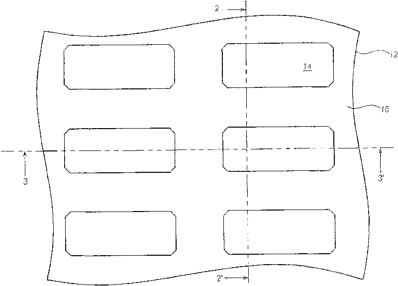
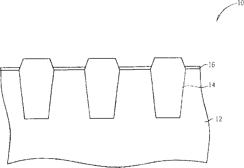
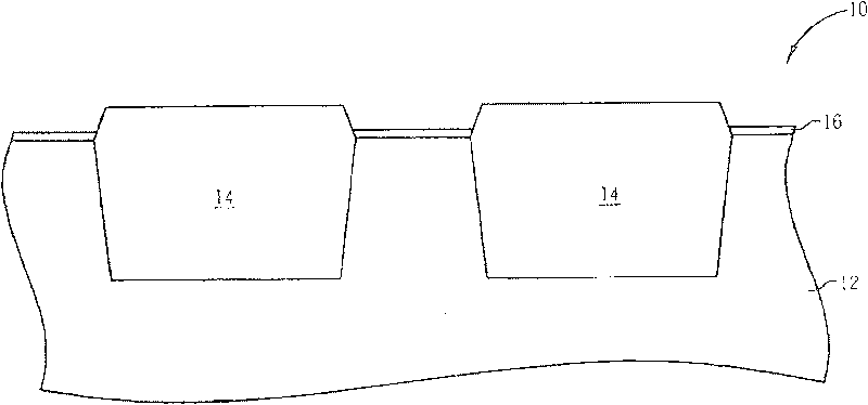
[0031] Please refer to FIGS. 9-19. FIGS. 9-19 are schematic diagrams of the process of the method for manufacturing the flash memory 50 of the present invention. In this embodiment, the flash memory 50 is a split-gate flash memory. First, a semiconductor substrate 52 is provided, which can be a silicon substrate, or a P-type or N-type silicon substrate. Picture 9 Only a partial area of ​​the semiconductor substrate 52 is shown, and Picture 10 for Picture 9 A schematic cross-sectional view of the semiconductor substrate 52 shown along the tangent line 10-10' (that is, the Y direction). Next, a plurality of insulating shallow trench structures 54 are formed on the surface of the semiconductor substrate 52. Since the upper surface of the insulating shallow trench structure 54 is higher than the surface of the semiconductor substrate 52, there is a recessed area 55 between adjacent insulating shallow trench structures 54 respectively. In addition, the semiconductor substrate 52...


PUM


Abstract

The invention provides a method for preparing a flash memory. Firstly, a semiconductor substrate is provided, then, an insulation shallow trench structure is prepared in the semiconductor substrate, and a floating gate dielectric layer is formed on the surface of the semiconductor substrate. After that, a first conductor layer and a grinding buffer layer are successively deposited on the semiconductor substrate, and a grinding process is carried out so as to remove a part of the conductor layer and the grinding buffer layer considering the insulation shallow trench structure as a stop layer. Then, the left grinding buffer layer is removed, and a dielectric layer, a control gate and a patterned cover layer are successively formed on the semiconductor substrate. Finally, the dielectric layerand the conductor layer which are not covered by a cover layer are removed so as to form a floating gate.

Description

Technical field [0001] The present invention provides a method for manufacturing a flash memory, in particular to a method for manufacturing a flash memory that uses a grinding method to avoid generating active area (AA) trenches. Background technique [0002] Non-volatile memory has the characteristic of not losing stored data due to power supply interruption, so it is widely used in information products. According to the number of data bits stored in a unit storage unit, the non-volatile memory can be divided into a single-bit storage non-volatile memory and a dual-bit storage non-volatile memory. The former includes Nitride Read-Only-Memory (NROM), Metal-Oxide-Nitride-Oxide-Silicon (MONOS) and other memory or silicon-oxide Silicon-Oxide-Nitride-Oxide-Silicon (SONOS) memory. The latter is, for example, a split-gate SONOS memory or a split-gate MONOS memory. Since the unit memory cells of the split-gate SONOS-type memory and the split-gate MONOS-type memory can store two bits...

Claims


Application Information

Patent Timeline
Patent Type & Authority Patents(China)
IPC IPC(8): H01L21/8247H01L21/336H01L21/28H01L21/321
Inventor 郭辉宏许正源刘世伟陈正智
Owner POWERCHIP SEMICON MFG CORP
Why Eureka
Try Eureka