


Quick Research
Generate reliable direction feasibility study reports for your R&D in just a few steps.

Technical Q&A
Discover and master advanced knowledge NOW. Basics, ideas, possibilities, all at once.

Find Solutions
As an expert in R&D theories, this can generate solutions to your technical problems instantly.

Evaluate Feasibility
Analyze your overall solution with one click, know your potential R&D risks in advance.

Monitor Landscape
Get weekly tech updates, stay abreast of the latest tech innovations and key insights.
Substrate of LCD device and manufacturing method thereof
A technology of a liquid crystal display device and a manufacturing method, which are applied in the directions of instruments, optics, nonlinear optics, etc., can solve the problems of affecting display quality, uneven response speed of liquid crystal display devices, and decreased contrast ratio, and achieve improved display quality and consistent response speed. , the effect of improving contrast
- Summary
- Abstract
- Description
- Claims
- Application Information
AI Technical Summary
Problems solved by technology
Method used
Image

Examples
Embodiment 1
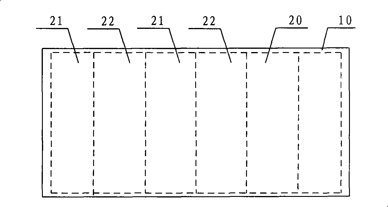
[0028] figure 1 It is a structural schematic diagram of Embodiment 1 of the present invention. Such as figure 1 As shown, the liquid crystal display device includes a substrate main body 10 and an alignment film 20 formed on the substrate main body 10. The alignment film 20 is composed of a first alignment film region 21 and a second alignment film region 22 arranged in sequence. The first alignment film region 21 and the second alignment film region 22 have different orientation characteristics, specifically: the first alignment film region 21 and the second alignment film region 22 are coated with different orientation materials, so that the first alignment film region 21 and the second alignment film region There is a set pencil hardness difference between the alignment film regions 22, and after subsequent rubbing treatment, there is a set orientation angle difference (hook angle difference) between the first alignment film region 21 and the second alignment film region 2...
Embodiment 2
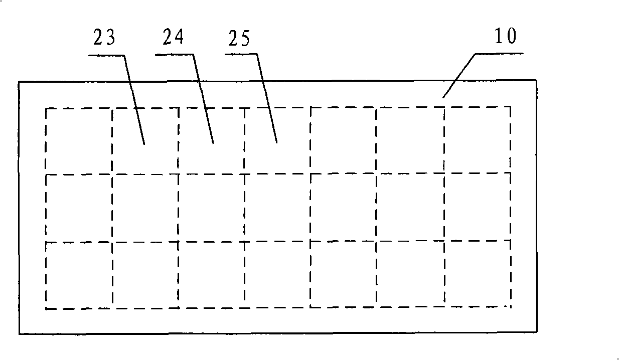
[0033] figure 2 It is a structural schematic diagram of Embodiment 2 of the present invention. Such as figure 2 As shown, the alignment film region may be a block alignment film region with one or several pixels as the unit, specifically: the third alignment film region 23, the fourth alignment film region 24, and the fifth alignment film region 25, each phase The adjacent alignment film regions are coated with different orientation materials, and each adjacent alignment film region has different orientation characteristics, specifically: there is a specific pencil hardness difference between the alignment film regions; There is a specific orientation angle difference between them. Among them, the alignment film regions with different orientation characteristics: the third alignment film region 23, the fourth alignment film region 24 and the fifth alignment film region 25 are respectively arranged above the colored resins of different colors, and the surface of the substra...
Embodiment 3
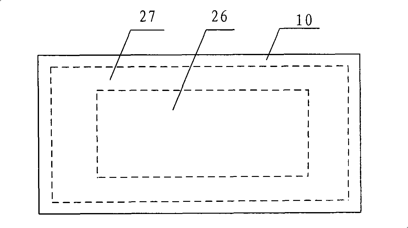
[0038] image 3 It is a structural schematic diagram of Embodiment 3 of the present invention. Such as image 3 As shown, the alignment film region is composed of a central alignment film region 26 and a peripheral alignment film region 27, and each alignment film region is coated with a different orientation material. Wherein, each alignment film area is coated with different orientation materials, and each alignment film area has different alignment characteristics, specifically: an alignment film with relatively good light transmission is formed in the middle alignment film area 26, and an alignment film with relatively good light transmission is formed in the peripheral area 26. The alignment film region 27 forms an alignment film with relatively poor light transmittance.
[0039] Due to the difference in the structure of the liquid crystal display device (for example, there is a sealant in the peripheral part and no sealant in the middle part), the central region and th...
PUM
 Abstract
Description
Claims
Application Information
 - R&D Engineer
- R&D Manager
- IP Professional
- Industry Leading Data Capabilities
- Powerful AI technology
- Patent DNA Extraction
Browse by: Latest US Patents, China's latest patents, Technical Efficacy Thesaurus, Application Domain, Technology Topic, Popular Technical Reports.
© 2024 PatSnap. All rights reserved.Legal|Privacy policy|Modern Slavery Act Transparency Statement|Sitemap|About US| Contact US: help@patsnap.com