
Patsnap Eureka
For R&D, Patsnap Eureka makes reading and utilizing patents & technical documents easy.
Patsnap Eureka AIR
Designed for self-driven R&D workflows. Generate viable solutions, solve complex R&D challenges, empower your innovation with AI.

Patsnap Eureka Materials
Designed for material experts only. Revolutionize your material R&D, from search, analyze, to developing new materials.

TechResearch
Generate reliable direction feasibility study reports for your R&D in just a few steps.

TechSeek
Discover and master advanced knowledge NOW. Basics, ideas, possibilities, all at once.

TechMind
As an expert in R&D Theories, TechMind can generates customized viable solutions instantly.

TechRisk
Analyze your overall solution with one click, know your potential R&D risks in advance.

TechMonitor
Get weekly tech updates, stay abreast of the latest tech innovations and key insights.
A method of manufacturing a structure
A mask, gold layer technology, applied in the field of manufacturing microelectronic devices with this structure, can solve the problems of limiting micro-contact printing, harmfulness, etc.
- Summary
- Abstract
- Description
- Claims
- Application Information
AI Technical Summary
Problems solved by technology
Method used
Image

Examples
Embodiment Construction
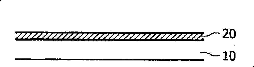
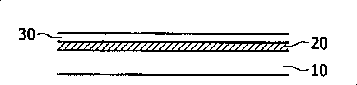
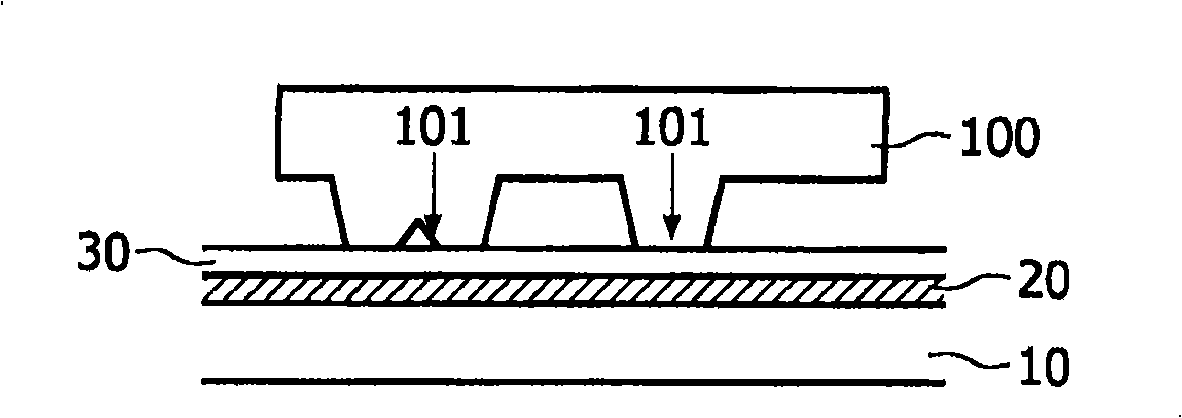
[0028] Figure 1 shows the six stages in a first embodiment of the method of the invention in cross-sectional view. Microcontact printing was used in this example for the patterning of the gold oxide layer. Therefore, patterning occurs after oxidation. More details are given in Examples 1-7.
[0029] Figure 1A A substrate 10 is shown with a gold layer 20 thereon. The substrate is a silicon substrate. The substrate has been thermally oxidized and provided with a Ti adhesion layer. Thereafter, the gold oxide layer 30 is provided by oxidizing the gold layer 20 in a plasma treatment ( Figure 1B ). Then, the gold oxide layer 30 is patterned using the stamp 100 ( Figure 1C). A stamp 100 suitable for microcontact printing has a stamp surface 101 conforming to a desired pattern. As is known to those skilled in the art, such a stamp is suitably fabricated from PDMS and any ink is provided to the stamp 100 prior to embossing. The ink includes a solvent with an active componen...
PUM
| Property | Measurement | Unit |
|---|---|---|
| critical temperature | aaaaa | aaaaa |
| electrical resistivity | aaaaa | aaaaa |
Abstract
Description
Claims
Application Information
 - R&D Engineer
- R&D Manager
- IP Professional
- Industry Leading Data Capabilities
- Powerful AI technology
- Patent DNA Extraction
Browse by: Latest US Patents, China's latest patents, Technical Efficacy Thesaurus, Application Domain, Technology Topic, Popular Technical Reports.
© 2024 PatSnap. All rights reserved.Legal|Privacy policy|Modern Slavery Act Transparency Statement|Sitemap|About US| Contact US: help@patsnap.com