
A device and method for FPGA simulation

A simulation and parameter configuration technology, applied in the field of data communication, can solve the problems of long verification time and low efficiency, and achieve the effects of simple error diagnosis, reduced processing time, and improved efficiency

Inactive Publication Date: 2011-04-06
曲亚平
View PDF0 Cites 0 Cited by
  • Summary
  • Abstract
  • Description
  • Claims
  • Application Information

AI Technical Summary

Problems solved by technology

[0013] The purpose of the present invention is to propose a method and device for FPGA simulation, which is mainly used to solve the problems of long time and low efficiency for FPGA logic simulation verification at present

Method used


Image

  • A device and method for FPGA simulation
  • A device and method for FPGA simulation
  • A device and method for FPGA simulation

Examples


Embodiment Construction

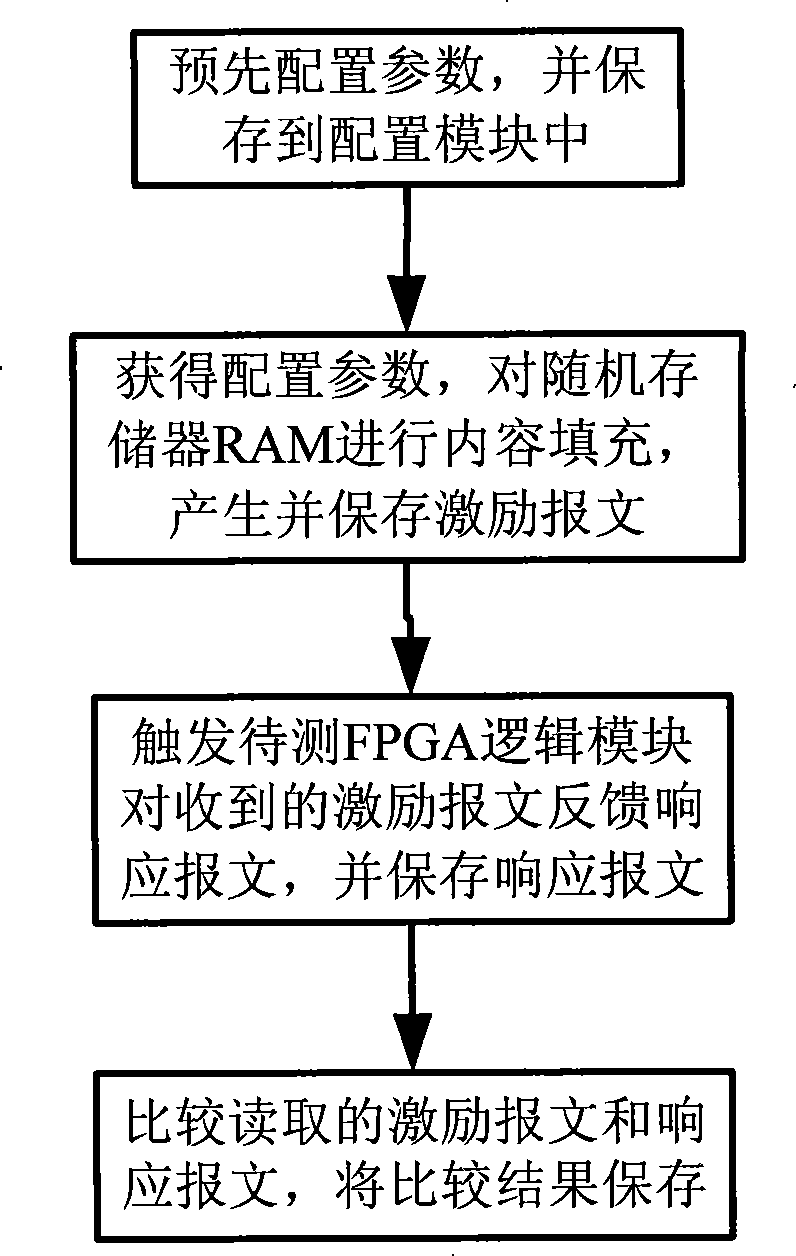
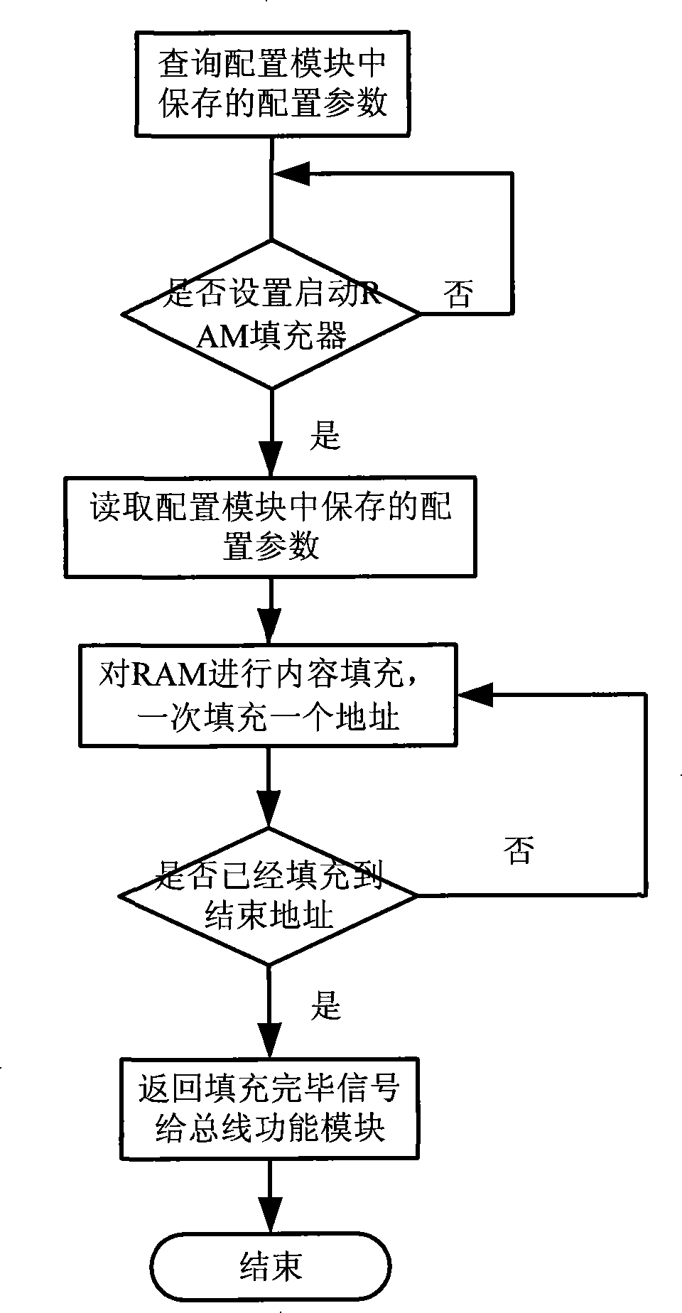
[0058] The basic technical idea of ​​the present invention is that when the FPGA logic module to be tested is simulated and verified, a RAM filling module is introduced to directly fill the content of the random access memory RAM according to random design requirements, without the need for the FPGA logic module to be tested according to the The timing requires reading and writing of preset data, which greatly reduces the time for simulation verification of the FPGA logic module to be tested, and greatly improves the efficiency of simulation verification of the FPGA logic module to be tested.

[0059] The present invention will be further described in detail below in conjunction with the accompanying drawings and specific embodiments.

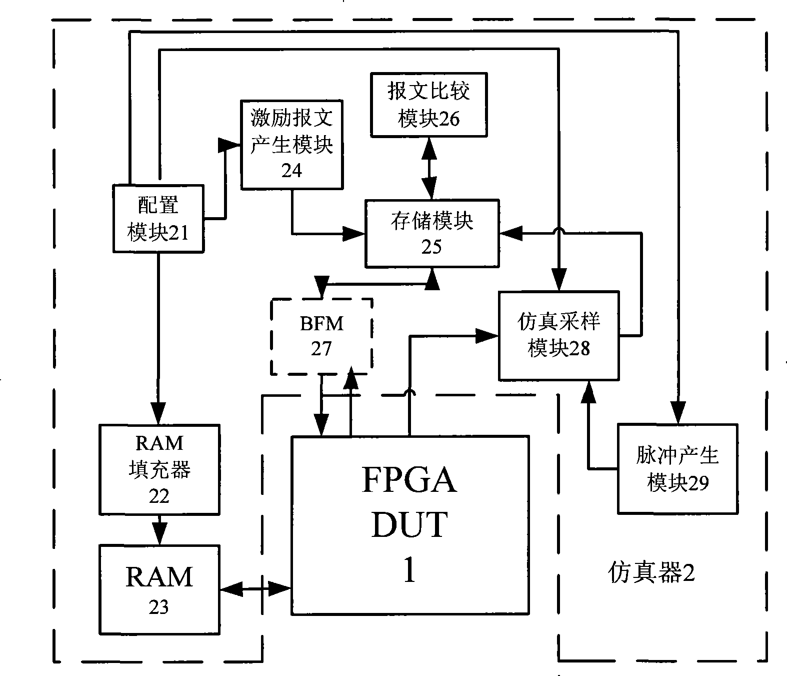
[0060] Such as figure 1 Shown is the structural diagram of a specific embodiment of the device of the present invention, comprises as shown in the figure: FPGA logic module to be tested (FPGA's DUT) 1 and emulator (TESTBENCH) 2, described FPGA ...


PUM


Abstract

The invention discloses an FPGA simulation device and a method thereof; the device comprises a configuration module configuring and conserving message parameters determined according to random design requirements, an incentive message generating module in inlet connection with the configuration module and used for generating and sending incentive messages to a memory module, a bus interface module connected with an FPGA logical module to be tested and providing interfaces and a bus required by the testing of the FPGA logical module, a message comparison module in inlet connection with the memory module and used for comparing incentive messages with the response messages input by the FPGA logical module to be tested and returning the comparative result to the memory module for conservation, together with an RAM stuffer in inlet connection with the configuration module and used for filling contents to the random access memory RAM. The FPGA simulation device and the method thereof greatly reduce the processing time for verifying the functions of a plurality of RAM interfaces of the FPGA logical module to be tested and enormously increase the efficiency of the FPGA logical simulation verification.

Description

technical field [0001] The present invention relates to the field of data communication, in particular to FPGA simulation technology, in particular to a device and method for FPGA simulation. Background technique [0002] With the development of data communication technology, especially the emergence of high-bandwidth and high-speed data communication technology, in the design of data communication chips, large-scale, high-speed, high-complexity data communication chip designs emerge in an endless stream, especially those based on FPGA. In large-scale logic design, the completed logic functions are numerous and complex. Usually, in order to ensure the reliability of the FPGA logic design in practical applications, the designed FPGA logic needs to be simulated and verified before it is put into use. In order to improve the efficiency of simulation, there are some devices specially used to verify and simulate the FPGA logic. . [0003] Existing verification simulation device...

Claims


Application Information

Patent Timeline
Patent Type & Authority Patents(China)
IPC IPC(8): H04L12/26H04L12/56
Inventor 刘一远
Owner 曲亚平
Learn More