Method and apparatus for assembling die on electronic substrate

A substrate and die technology, applied in circuits, electrical components, electrical solid devices, etc., can solve the problems of reducing the degree of plastic deformation strain, reducing the life cycle of the die package, etc., to achieve the effect of reducing the life cycle

Inactive Publication Date: 2008-09-03
GLOBALFOUNDRIES INC
View PDF0 Cites 2 Cited by
  • Summary
  • Abstract
  • Description
  • Claims
  • Application Information

AI Technical Summary

Problems solved by technology

[0009] Furthermore, conventional methods do not provide a means to enhance the predicted life cycle of self-standing components by halving the peak stress
Reduction in peak stress during temperature cycling reduces the degree of plastic deformation strain which is known to reduce die package life cycle

Method used


Image

  • Method and apparatus for assembling die on electronic substrate
  • Method and apparatus for assembling die on electronic substrate
  • Method and apparatus for assembling die on electronic substrate

Examples


Embodiment Construction

[0039] Referring now to the drawings, and in particular to Figures 1-18b, there are shown exemplary embodiments of methods and structures in accordance with the present invention.

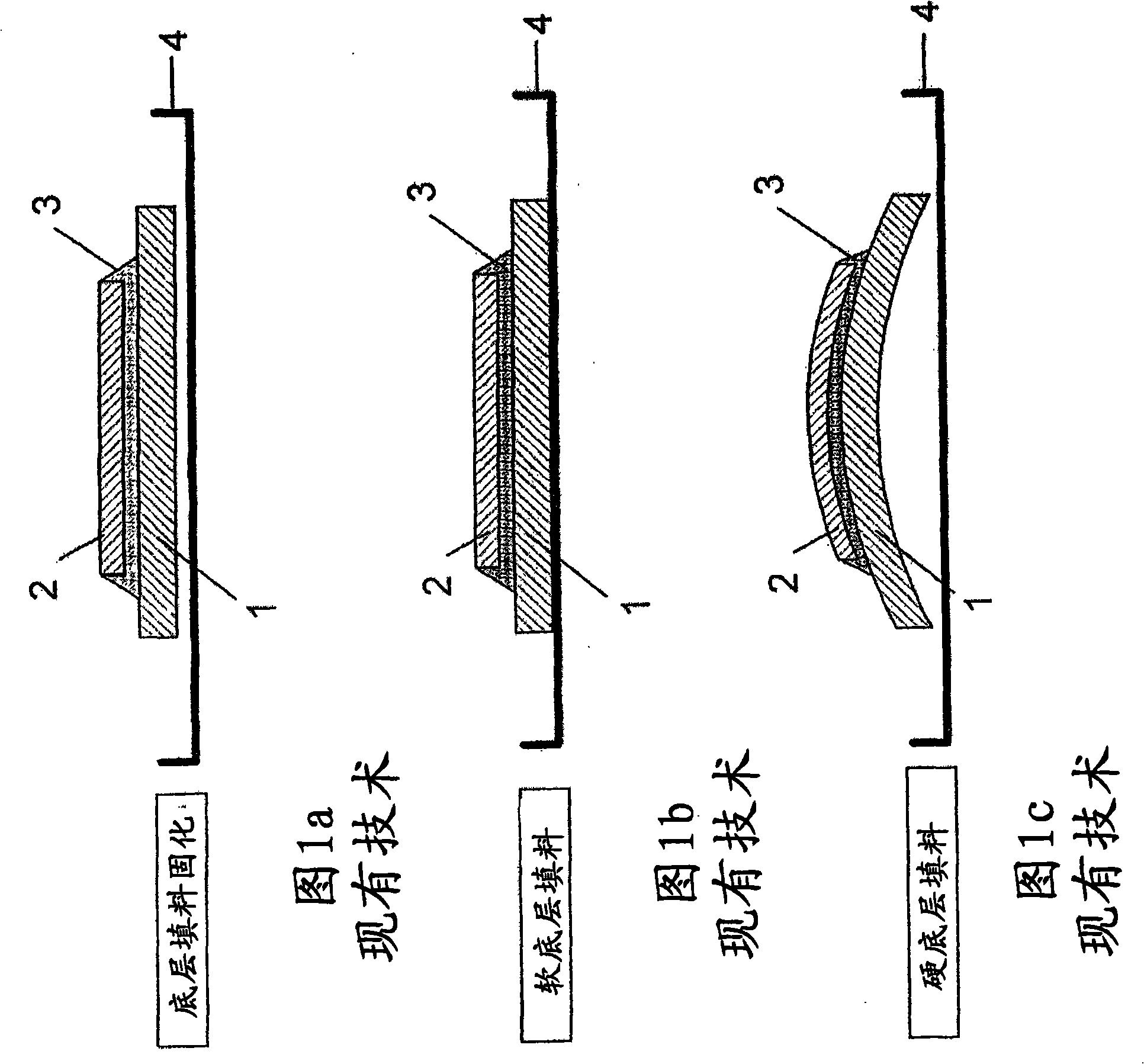
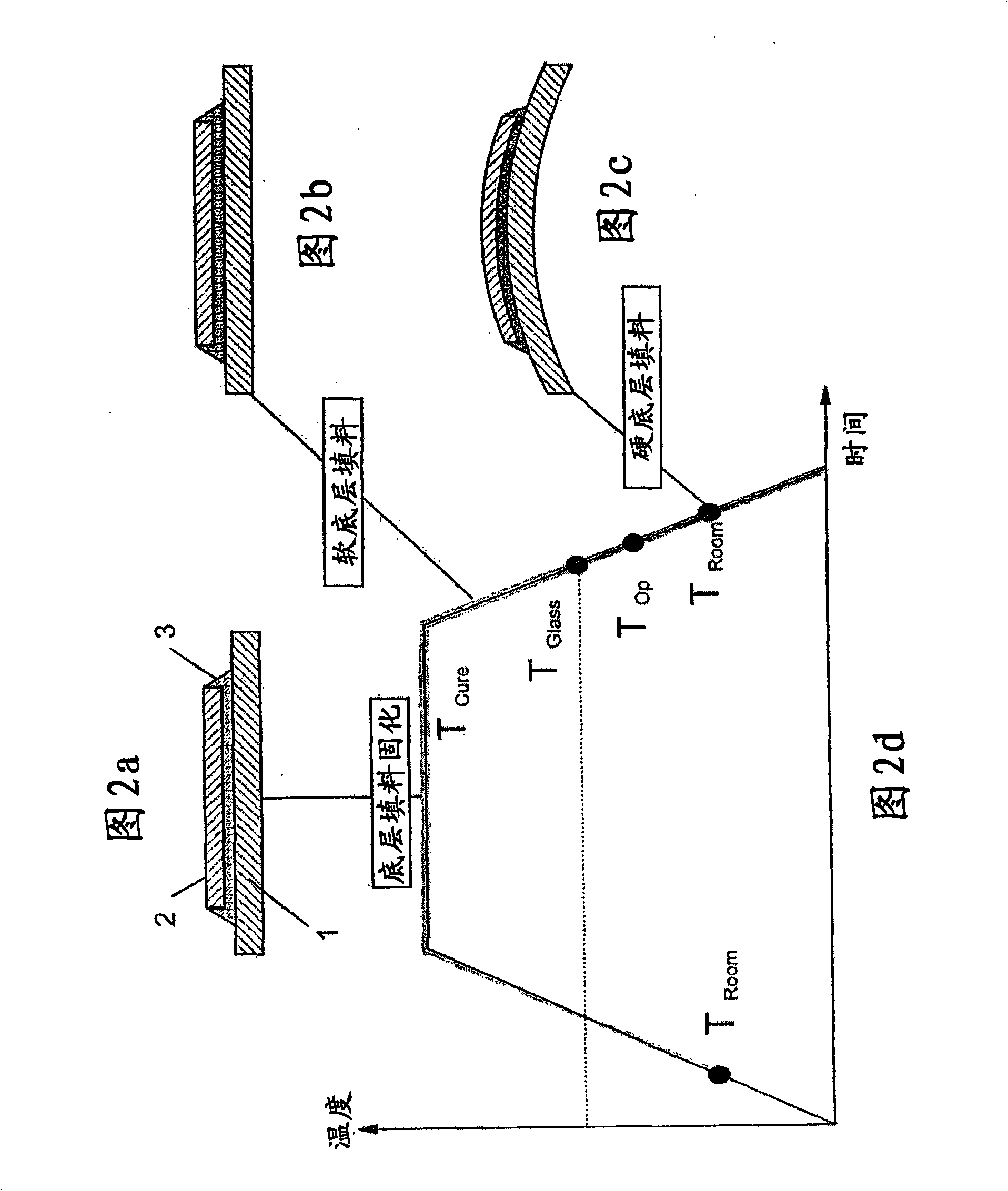
[0040] Figures 1a-1c illustrate the three stages of a die 2 / substrate 1 / underfill 3 assembly during a curing cycle. The substrate 1 and die (chip) 2 that have been bonded by the reflow process are injected with an underfill 3 and placed in a tray 4 .

[0041] Figure 1 a shows the underfill 3 being soft at the start of the curing process, during which the underfill 3 hardens thermally as it cures. Underfill 3 at its glass transition temperature (T glass ) above are generally soft. As the glass transition temperature is crossed, as shown in Figure 1b, at the glass transition temperature (T glass ), the hardened underfill 3 essentially locks the substrate 1 and the silicon (die 2) in their freely expanded state.

[0042] As the package is cooled, the substrate 1 (eg, with a 5×CTE) is more than fiv...


PUM


Abstract

A method (and apparatus) of assembling a die on an electronic substrate, includes processing an assembly including a substrate and a die, and during the processing, introducing a pre-stress to the assembly during a cure process.

Description

technical field [0001] The present invention generally relates to methods and apparatus for fabricating electronically integrated chips with enhanced thermomechanical characteristics. technical background [0002] Conventional electronic packaging utilizes ceramic substrates to support silicon dies, however, ceramic packaging comes at a higher cost. The coefficients of thermal expansion (CTE) of both the silicon die and the ceramic are very close (approximately 3ppm / °C), so that temperature excursions make these components stretch uniformly. However, any CTE differences subject to temperature changes can cause shear and other forms of stress in the solder ball connection (referred to as C4). In addition, cyclic stress can reduce the lifetime (ie, service life) of the C4 connection, with 0-pk values ​​of C4 stress and substrate stress substantially contributing to package lifetime. [0003] The current trend is towards low-cost organic substrates with superelectric properti...

Claims


Application Information

Patent Timeline
Patent Type & Authority Applications(China)
IPC IPC(8): H01L21/50H01L21/58H01L21/60
CPCH01L21/563H01L24/75H01L24/81H01L24/83H01L24/92H01L2224/13111H01L2224/73203H01L2224/75704H01L2224/81815H01L2924/01013H01L2924/01033H01L2924/01082H01L2924/14H01L2924/19041H01L2924/19043H01L2924/3511H01L2224/131H01L2224/2919H01L2924/01006H01L2924/01019H01L2924/0105H01L2924/014H01L2924/0665H01L2924/00013H01L2924/10253H01L2224/83H01L2924/15787H01L2924/00014H01L2924/00011H01L2924/01014H01L2924/00H01L2924/3512H01L2224/29099H01L2224/0401
Inventor 斯里·M·斯里-加扬塔
Owner GLOBALFOUNDRIES INC
Why Eureka
Try Eureka