Eureka AIR delivers breakthrough ideas for toughest innovation challenges, trusted by R&D personnel around the world.

Method for measuring semiconductor quantum point dimension distribution using fluorescence spectrum

A technology of size distribution and fluorescence spectrum, which is applied in the field of measuring the size distribution of semiconductor quantum dots by fluorescence spectrum, can solve problems such as the complexity of the detection process, and achieve the effects of simple operation, good product quality, and short time consumption

Inactive Publication Date: 2008-08-27
SHANGHAI INST OF TECHNICAL PHYSICS - CHINESE ACAD OF SCI
View PDF0 Cites 2 Cited by
  • Summary
  • Abstract
  • Description
  • Claims
  • Application Information

AI Technical Summary

Problems solved by technology

At present, the commonly used detection methods include atomic force microscope, high-resolution transmission electron microscope, etc. The disadvantage of these methods is that the detection process is complicated

Method used


Image

  • Method for measuring semiconductor quantum point dimension distribution using fluorescence spectrum
  • Method for measuring semiconductor quantum point dimension distribution using fluorescence spectrum
  • Method for measuring semiconductor quantum point dimension distribution using fluorescence spectrum

Examples


Embodiment Construction

[0021] Below by embodiment and accompanying drawing, the present invention is described in further detail:

[0022] 1. In this embodiment, InAs / GaAs quantum dot samples are used, and the PL spectrum is first measured, and the measurement conditions are:

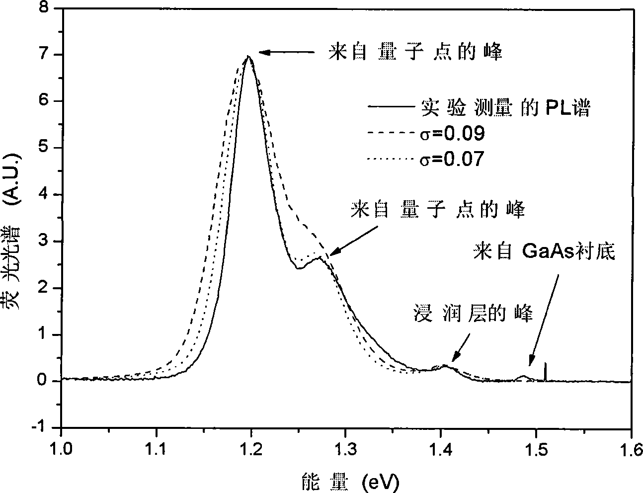
[0023] The quantum dot sample is placed under the objective lens of the microfluorescence spectrometer, the measurement temperature is controlled at a low temperature of 80K, the incident laser power is 200mW, and the incident laser wavelength is 632.8nm. At this time, the carrier density formed in the quantum dot sample is about 1.6×10 16 cm -3 , measured the PL spectrum of the InAs / GaAs quantum dot system, see figure 1 The solid line in , it can be seen that the center position of the peak of the PL spectrum (E 0 ) is 1.24eV, and the half-peak width is 75meV.

[0024] 2. Calculate the PL spectrum of the system according to the above-mentioned theoretical calculation method of InAs / GaAs semiconductor quantum dot PL spect...


PUM


Abstract

The invention discloses a method for utilizing fluorescence spectrums to measure size distribution of quantum dots of a semiconductor. The method obtains the size distribution of the quantum dots through field measurement of PL spectrums of a multiple quantum dot system of the semiconductor, calculation of the PL spectrums of the quantum dots of the semiconductor beginning from a time-dependent perturbation Schrodinger equation with approximate active mass, and then through theoretical and experimental PL spectrum contrast, wherein, the central wavelength of the PL spectrums corresponds to composite luminescence of a quantum dot with the largest ratio, and the shape of the PL spectrums corresponds to size distribution rules. The method for utilizing the fluorescence spectrums to measure the size distribution of the quantum dots of the semiconductor is simple and convenient in operation and short in time consumption, and can clearly and definitely obtain the size distribution of the multiple quantum dot system of the semiconductor.

Description

technical field [0001] The invention relates to a method for measuring the size distribution of InAs / GaAs or InAs / InP semiconductor quantum dots by using fluorescence spectrum. Background technique [0002] The self-organized growth mode is currently the more commonly used quantum dot growth method. In practical device applications, in order to optimize the performance of optoelectronic devices such as quantum dot lasers and quantum dot detectors, a high-density multi-layer multi-quantum dot system growth method is generally used. Because this method is difficult to grow a multi-quantum dot system with uniform size, the PL spectrum of quantum dots does not show the characteristics of delta function, but shows a certain broadening, which hinders the application of quantum dot optoelectronic devices to a certain extent. performance. For this reason, some people use different orientations and patterned substrates and optimize the growth process, which improves the uniformity ...

Claims


Application Information

Patent Timeline
Patent Type & Authority Applications(China)
IPC IPC(8): G01N21/64G01B11/00G06F17/10
Inventor 陆卫杨希峰陈平平李天信甄红楼张波李宁李志锋陈效双
Owner SHANGHAI INST OF TECHNICAL PHYSICS - CHINESE ACAD OF SCI
Why Eureka
Eureka Blog
Learn More