
Semiconductor integrated circuit and multi-chip module

A technology of integrated circuits and semiconductors, applied in the direction of semiconductor devices, circuits, semiconductor/solid-state device components, etc., can solve the problems of reducing the area, weakening the area reduction effect, etc.

Active Publication Date: 2008-05-14
SOCIONEXT INC
View PDF0 Cites 5 Cited by
  • Summary
  • Abstract
  • Description
  • Claims
  • Application Information

AI Technical Summary

Problems solved by technology

[0008] However, in the above-mentioned conventional semiconductor integrated circuit in which pads are provided in two stages, as shown in FIG. In a semiconductor integrated circuit in which pads are set to two levels, for example, when there are five redundant pads, if five redundant pads 2 are provided, as shown by the dotted line in FIG. 26, the area will increase accordingly. The area required for the setup of 5 redundant pads 2, thereby weakening the area reduction effect

Method used


Image

  • Semiconductor integrated circuit and multi-chip module
  • Semiconductor integrated circuit and multi-chip module
  • Semiconductor integrated circuit and multi-chip module

Examples


no. 1 Embodiment approach

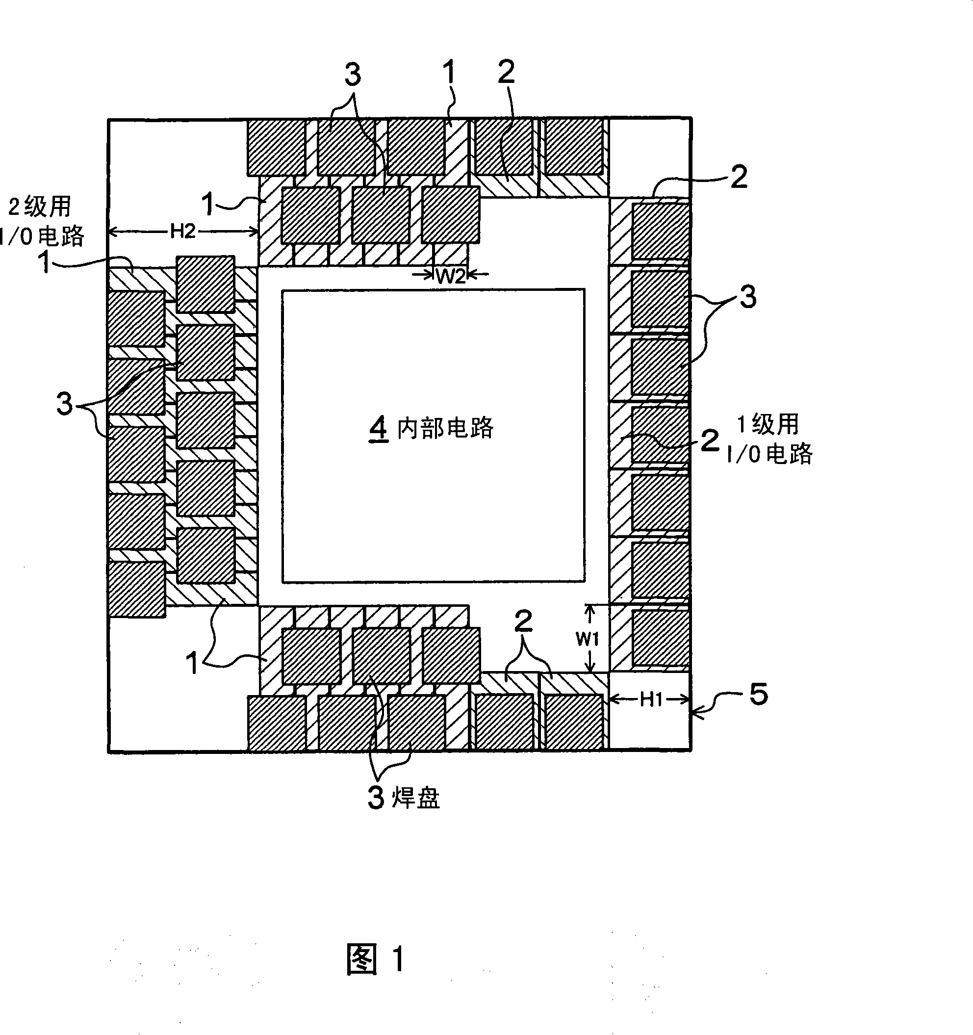
[0077] FIG. 1 shows the semiconductor integrated circuit of this embodiment.

[0078] A semiconductor integrated circuit 5 serving as a semiconductor chip in the figure has a rectangular shape, and an internal circuit 4 is provided in the center. On the outside of the above-mentioned internal circuit 4, a plurality of I / O circuits 1, 2 are provided along the four sides of the outer periphery. These I / O circuits are used to output signals of the internal circuit 4 to the outside or input external signals to the internal circuit 4, and the pads 3 are provided thereon.

[0079] There are two kinds of the above-mentioned plurality of I / O circuits. The I / O circuit 1 is an I / O circuit for m (m=2) stages in which two pads 3 can be arranged in a direction facing the above-mentioned internal circuit 4. The O circuit 2 is an I / O circuit for n (n=1 (n

no. 2 Embodiment approach

[0089] Next, a second embodiment of the present invention will be described.

[0090] FIG. 8 shows the semiconductor integrated circuit of this embodiment. In this semiconductor integrated circuit, the I / O circuit 1 for the second stage is provided on the upper side, the lower side, and the left side, and the I / O circuit 2 for the first stage is provided on the right side. At the corners C of the lower right part and the upper right part of the semiconductor integrated circuit 5, there are provided power supply wirings for switching the power supply wiring between the I / O circuit 2 for the first stage and the I / O circuit 1 for the second stage. Transit area A. That is, in other words, the present embodiment adopts a structure in which the same type of I / O circuits are provided on each side of the semiconductor integrated circuit 5, and does not change the type of I / O circuits from one side to two levels on one side. For level use or from level 2 use to level 1 use, change th...

no. 3 Embodiment approach

[0095] Next, a third embodiment of the present invention will be described.

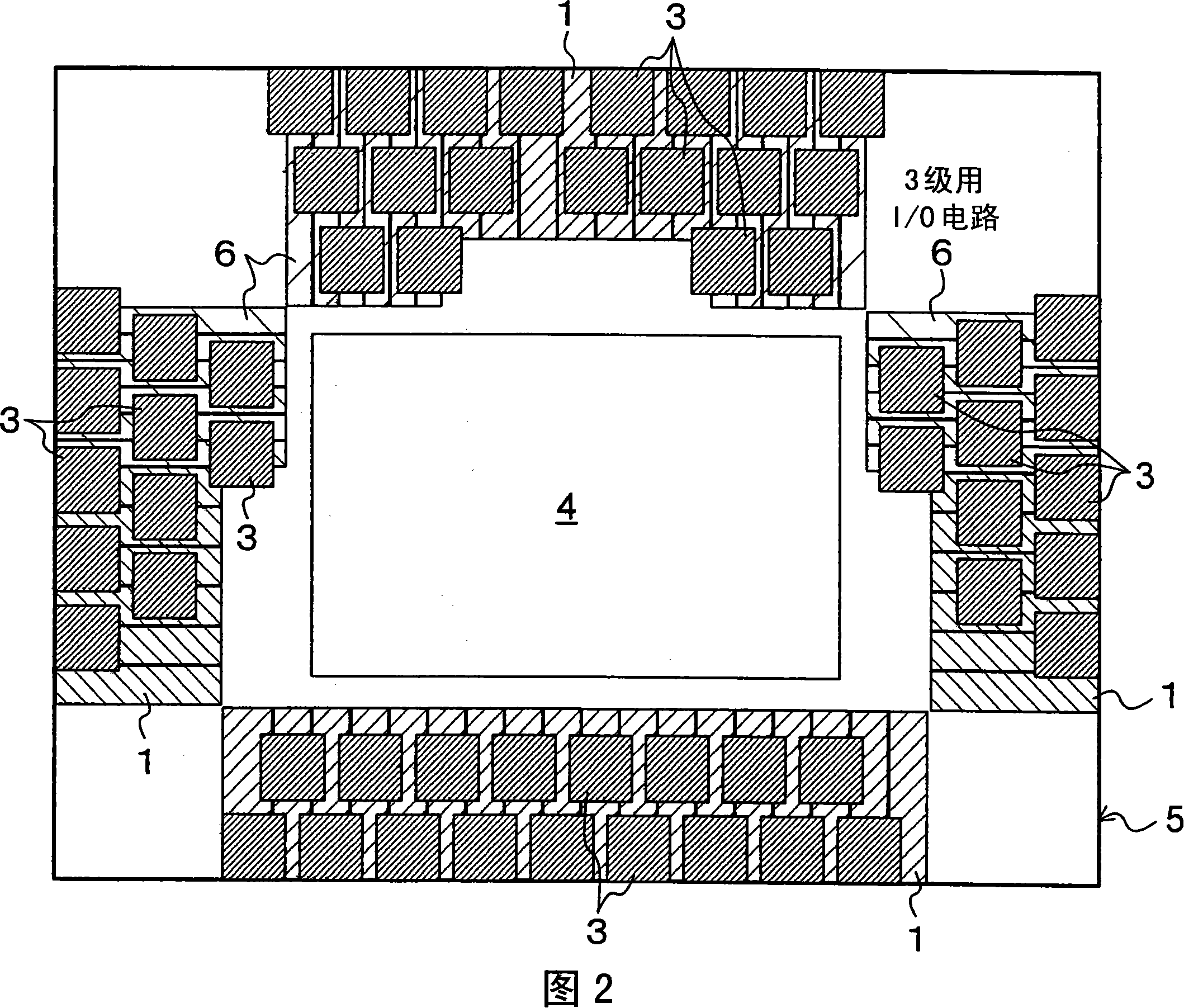
[0096] FIG. 12 shows the semiconductor integrated circuit of this embodiment. FIG. 13 shows a view after the pad 3 is removed from the structure of the semiconductor integrated circuit of FIG. 12 . This embodiment takes into account the ease of wire connection when the semiconductor integrated circuit is mounted in a semiconductor package.

[0097] In the semiconductor integrated circuit 5 in the figure, the I / O circuits 2 for the first stage are arrayed on the opposite sides of the upper and lower sides, and the I / O circuits 1 for the second stage are arrayed on the opposite sides of the left and right sides. . Therefore, the power wiring transition area A is provided on all four corners. In other words, the first-level I / O circuits 2 and the second-level I / O circuits 1 are adjacent to each other at each corner, and the second-level I / O circuits 1 are not adjacent to each other.

[0098] Therefo...


PUM


Abstract

An internal circuit is arranged in the center portion of a semiconductor integrated circuit, and a plurality of two kinds of I / O circuits (1,2)for inputting and outputting signals from and to the outside and many pads are arranged along four sides of the semiconductor integrated circuit. The I / O circuits (2)are one of the foregoing two kinds are one-pad I / O circuits. The plurality of I / O circuits(1)that are of the other of the foregoing two kinds are two-pad I / O circuits on which two pads are arranged in zigzag relationship in a direction toward the internal circuit. The number of arranged pads equals to the number of pads required for the semiconductor integrated circuit. The one-pad I / O circuits and the two-pad I / O circuits are provided with power source wirings for supplying power thereto. The power source wirings extend along the arrangement direction of the one-pad I / O circuits and the second-pad I / O circuits to be ring-shaped. The power source wiring migration areas for changing power source wirings between the one-pad I / O circuits and second-pad I / O circuits are disposed in four corner portions of the semiconductor integrated circuit, thereby minifying the areas even in the semiconductor integrated circuit with more pads.

Description

technical field [0001] The present invention relates to a semiconductor integrated circuit having I / O circuits and pads, which are interfaces with the outside, on the peripheral portion, and more particularly to a semiconductor integrated circuit whose number of pads is relatively small relative to the scale of the internal circuit. Many semiconductor integrated circuits. Background technique [0002] Conventionally, in a semiconductor integrated circuit as a semiconductor chip, as shown in FIG. [0003] In recent years, in response to the miniaturization of the process, more functions than before can be provided in one semiconductor integrated circuit, and the number of I / O circuits and pads provided as an interface with the outside is also increasing. However, low-voltage transistors used in memory circuits and logic circuits, and high-voltage transistors used in analog circuits and I / O circuits, etc., have different effects of area reduction due to miniaturization. Comp...

Claims


Application Information

Patent Timeline
IPC IPC(8): H01L27/02H01L23/50
CPCH01L2224/06153H01L2924/14H01L24/06H01L2224/05554
Inventor 松冈大辅
Owner SOCIONEXT INC
Learn More