Liquid crystal device and electronic apparatus
A technology of liquid crystal device and liquid crystal layer, applied in nonlinear optics, instrumentation, optics, etc.
- Summary
- Abstract
- Description
- Claims
- Application Information
AI Technical Summary
Problems solved by technology
Method used
Image
Examples
no. 1 approach
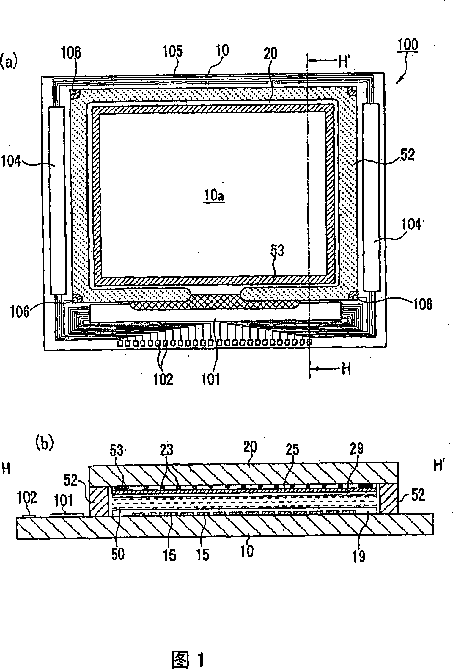
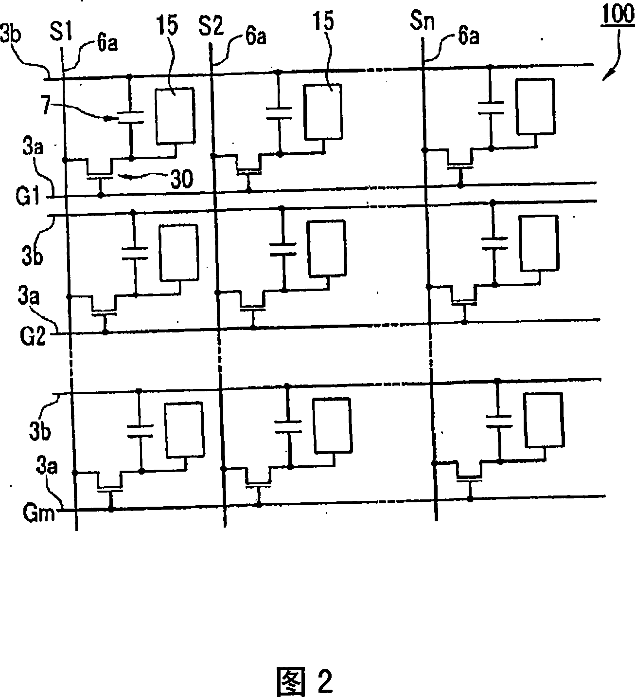
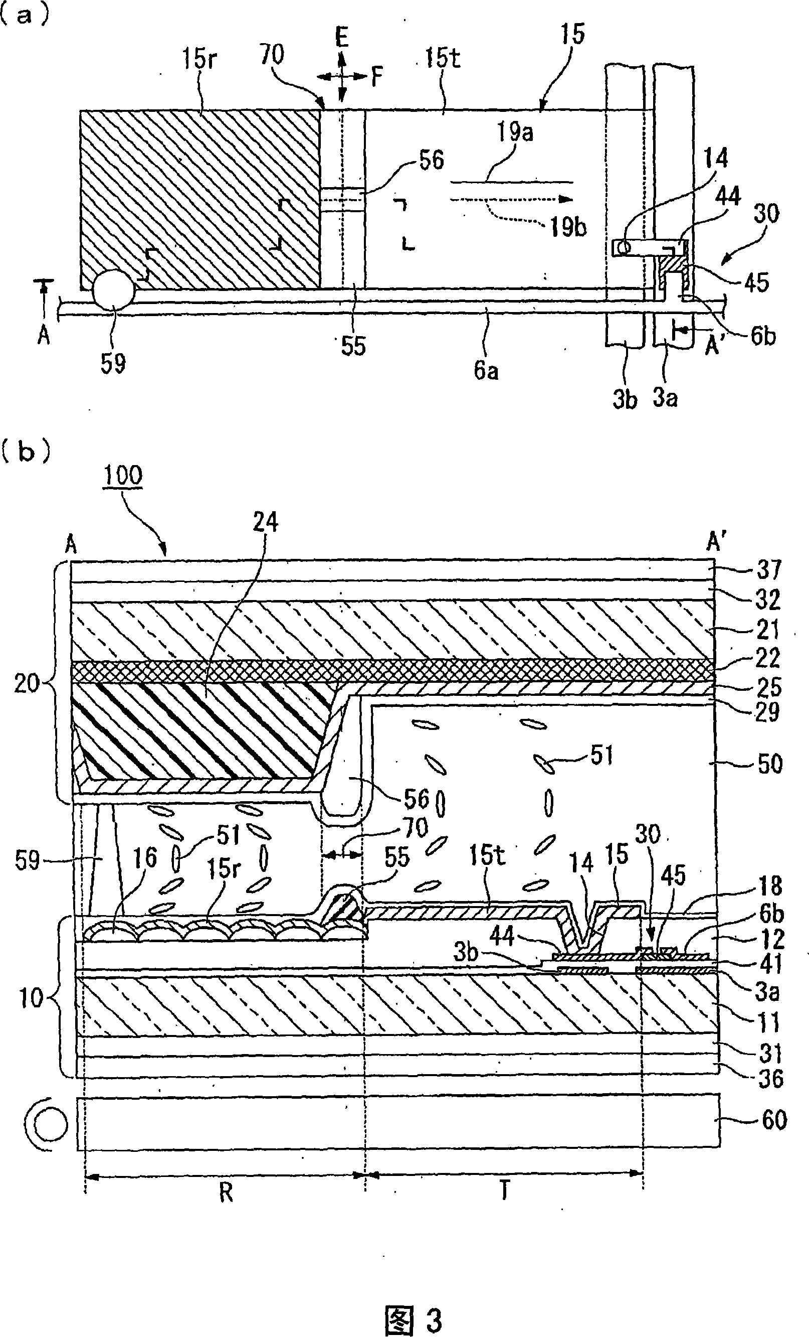
[0039] First, a liquid crystal device according to a first embodiment of the present invention will be described with reference to FIGS. 1 to 4 .
[0040] The liquid crystal device of this embodiment is an active matrix liquid crystal device using TFT elements as pixel switching elements. Moreover, as shown in FIG. 3 , it is a transflective liquid crystal device of a so-called multigap type, which includes a TFT array substrate 10 (first substrate), and is arranged opposite to the TFT array substrate 10 and placed in front of the observer. The opposite substrate 20 (second substrate) on the side, the liquid crystal layer 50 sandwiched between the substrates 10, 20, and the reflective electrode 15r provided on the TFT array substrate 10 to reflect light incident from the opposite substrate 20 side , and liquid crystal layer thickness adjustment for making the layer thickness of the liquid crystal layer 50 in the reflective display region R where the reflective electrode 15r exist...
no. 2 approach
[0075] Next, a second embodiment of the present invention will be described.
[0076] The basic configuration of the liquid crystal device of this embodiment is the same as that of the first embodiment. The difference is that, in the first embodiment, a pair of initial transfer structures are arranged at positions overlapping with the plane of the pixel electrode, but in contrast to this, in this embodiment, a pair of initial transfer structures are arranged at positions not overlapping with the plane of the pixel electrode. Initial transfer construct. Therefore, only this point of difference will be described below.
[0077] For the liquid crystal device of the present embodiment, for example, the liquid crystal device of the form illustrated in FIGS. 5( a ), ( b ), FIGS. The pair of initial transfer structures are arranged in a position not planarly coincident with the pixel electrode 15 , that is, an area outside the so-called display area. Among them, the "display area"...
PUM
 Abstract
Description
Claims
Application Information
 - R&D
- Intellectual Property
- Life Sciences
- Materials
- Tech Scout
- Unparalleled Data Quality
- Higher Quality Content
- 60% Fewer Hallucinations
Browse by: Latest US Patents, China's latest patents, Technical Efficacy Thesaurus, Application Domain, Technology Topic, Popular Technical Reports.
© 2025 PatSnap. All rights reserved.Legal|Privacy policy|Modern Slavery Act Transparency Statement|Sitemap|About US| Contact US: help@patsnap.com


