Method for manufacturing circuit forming board
A manufacturing method and substrate technology, applied in multilayer circuit manufacturing, printed circuit manufacturing, printed circuit and other directions, can solve problems such as difficult circuit positioning, poor quality reliability, etc., to improve production capacity, improve reliability, and improve finished products. rate effect
- Summary
- Abstract
- Description
- Claims
- Application Information
AI Technical Summary
Problems solved by technology
Method used
Image

Examples
no. 1 approach
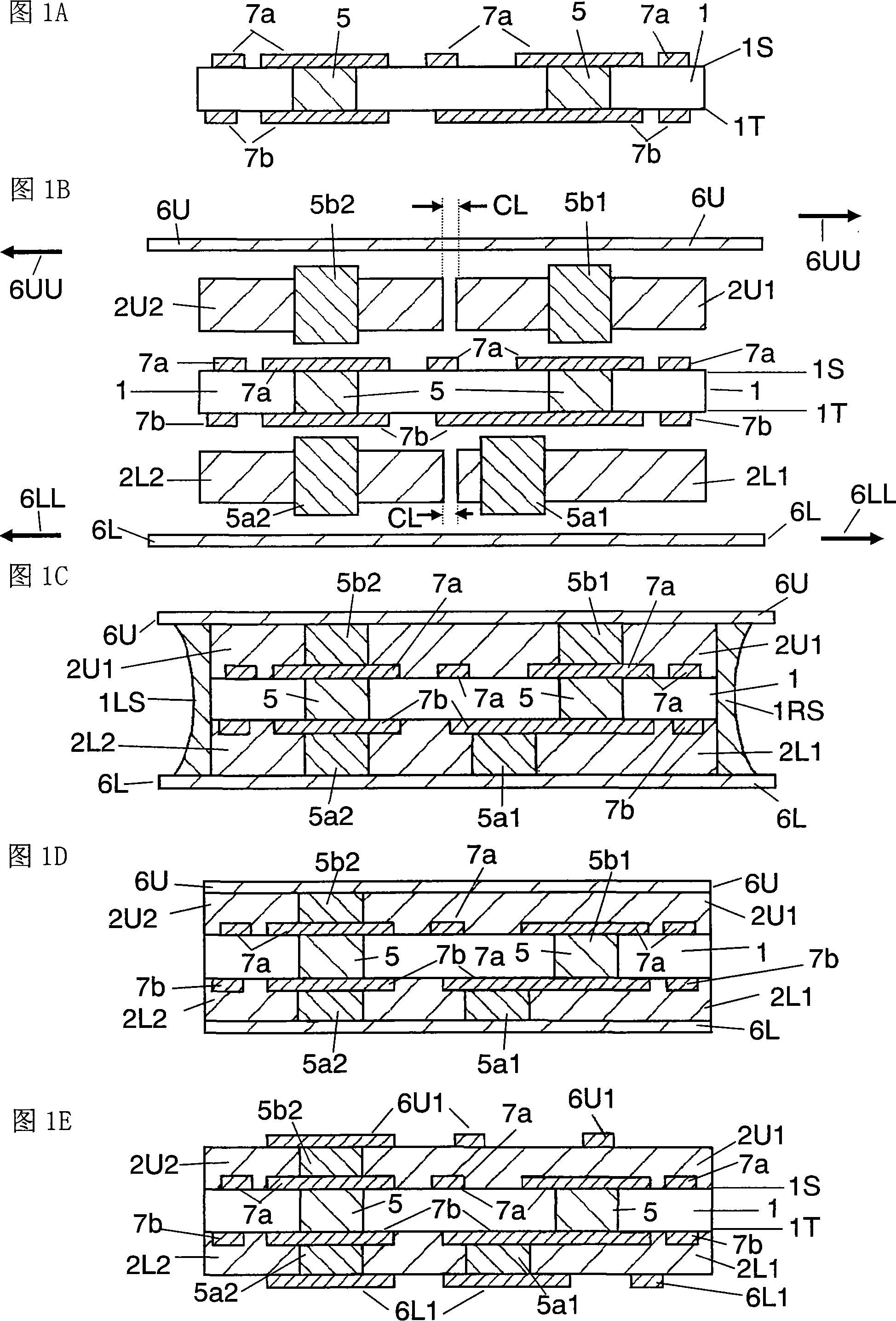
[0088] 1A to 1E are cross-sectional views illustrating a method of manufacturing a circuit-formed substrate according to a first embodiment of the present invention.
[0089]A circuit 7a is formed on one main surface 1S of the core substrate material 1 shown in FIG. 1A. Another circuit 7 b is formed on the other main surface 1T of the core substrate material 1 . Although the core substrate material 1 is shown as a double-sided board provided with a conductive paste 5 as an interlayer connection, a multilayer circuit substrate may also be used. In the so-called interlayer connection portion for connecting the circuit 7a on the side of one main surface 1S and the circuit 7b on the side of the other main surface 1T, in addition to the conductive paste 5, various types of plating, soldering, etc. not shown can also be used. various methods.
[0090] The core substrate material 1 has a C-stage. In the present invention, the C state means a cured state. In addition, the followin...
no. 2 approach
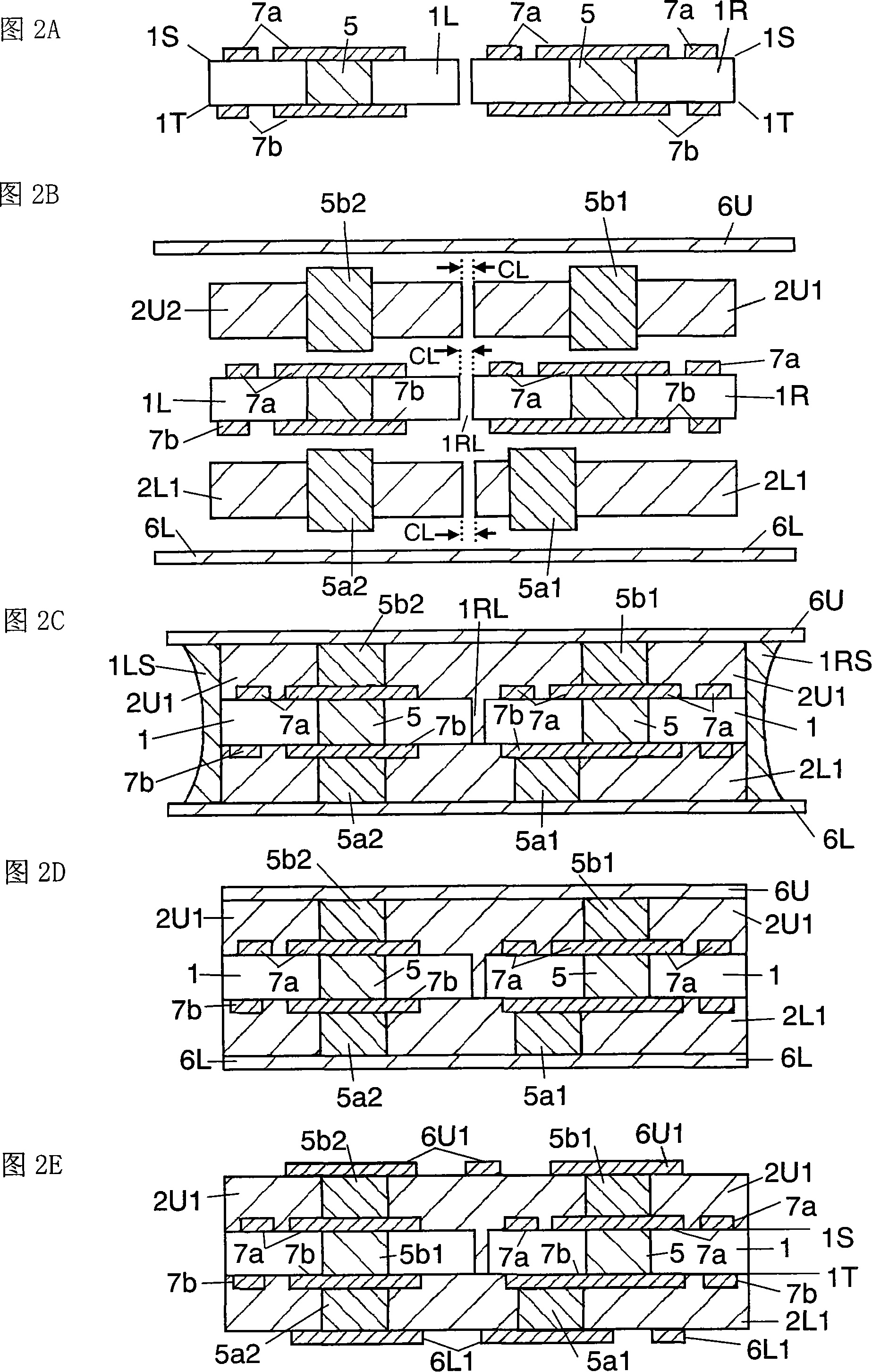
[0105] 2A to 2E are cross-sectional views illustrating a method of manufacturing a circuit-formed substrate according to a second embodiment of the present invention. The overall manufacturing process shown in the second embodiment is basically the same as that in the first embodiment. The big difference is that, in addition to dividing the film, the core substrate material 1 is also divided.
[0106] In FIG. 2A there are shown two core substrate materials 1R, 1L. The structure in which the core substrate material is divided into two is different from that of the first embodiment. Circuits 7a, 7b are formed on one main surface 1S and the other main surface 1T of core substrate materials 1R, 1L, respectively. Although the core substrate materials 1R, 1L are shown as double-sided substrates provided with conductive paste 5 as an interlayer connection portion for connecting the circuit 7a and the circuit 7b, a multilayer substrate may also be used. For the interlayer connectio...
no. 3 approach
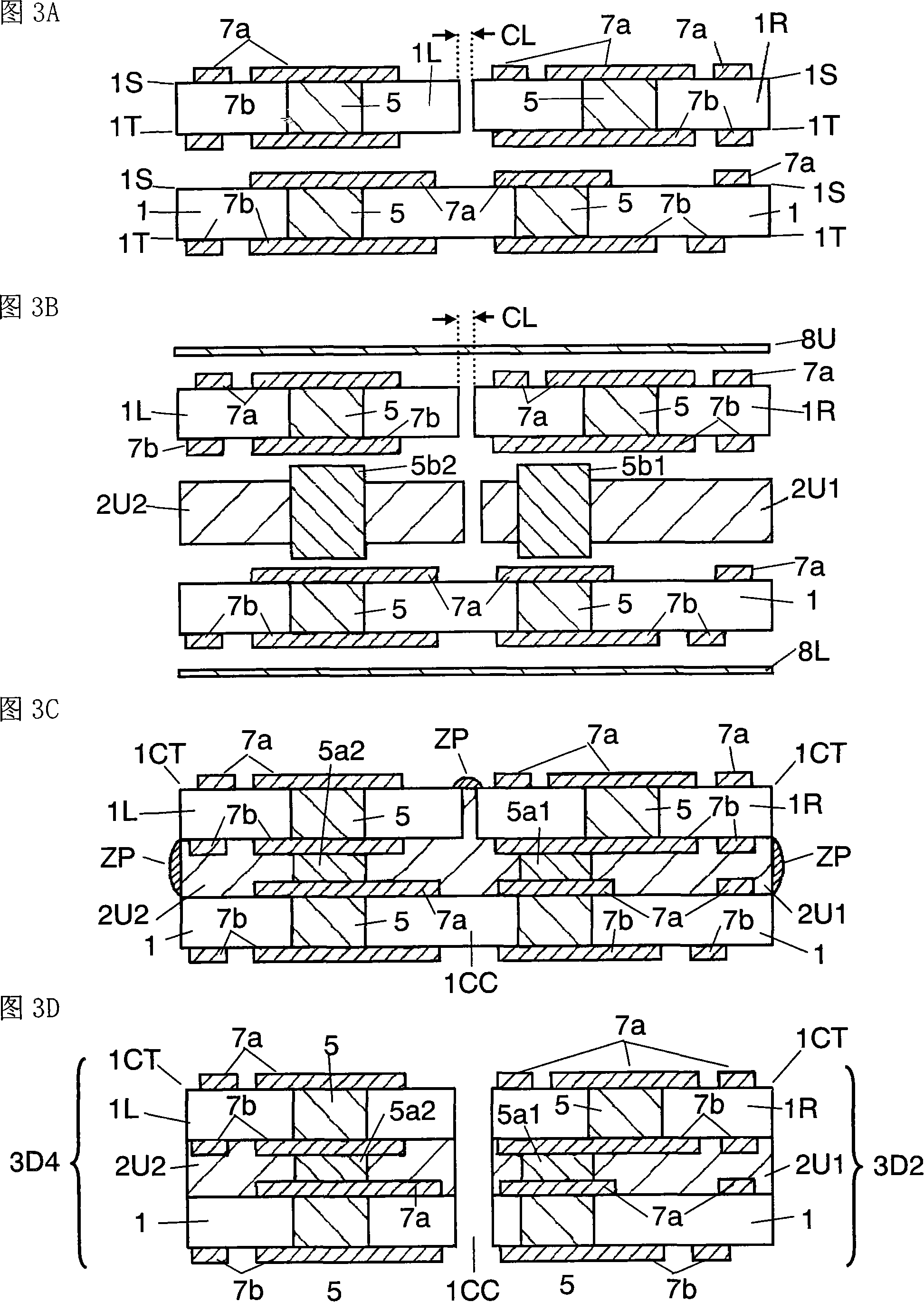
[0119] A third embodiment of the present invention will be described using FIGS. 3A to 3D .
[0120] As shown in FIG. 3A , two sets of core substrate materials 1 are prepared. One group represents core substrate materials 1R and 1L on the upper side in the figure. These core substrate materials are the same as those shown in the second embodiment, and are divided into two pieces. The other group is the core substrate material 1 on the lower side. The core substrate material 1 is basically the same as that shown in the first embodiment. That is, it can be said that the core substrate material in the third embodiment has a combined structure of the first embodiment and the second embodiment.
[0121] Circuits 7 a are formed on one main surface 1S of the core substrate materials 1 , 1R, and 1L, respectively. Circuits 7 b are each formed on the other main surface 1T of the core substrate materials 1 , 1R, and 1L. The electric circuit 7 a and the electric circuit 7 b are conne...
PUM
 Abstract
Description
Claims
Application Information
 - Generate Ideas
- Intellectual Property
- Life Sciences
- Materials
- Tech Scout
- Unparalleled Data Quality
- Higher Quality Content
- 60% Fewer Hallucinations
Browse by: Latest US Patents, China's latest patents, Technical Efficacy Thesaurus, Application Domain, Technology Topic, Popular Technical Reports.
© 2025 PatSnap. All rights reserved.Legal|Privacy policy|Modern Slavery Act Transparency Statement|Sitemap|About US| Contact US: help@patsnap.com