Antenna and wireless communication device

A technology for antennas and antenna parts, applied to antennas, resonant antennas, electrical short antennas, etc., can solve problems such as the inability to change the third resonant frequency, the inability to meet low voltage, and the inability to change the resonant frequency to achieve low control voltage and realize Effects of Broadband and Multi-Resonance

Active Publication Date: 2008-01-23
MURATA MFG CO LTD
View PDF3 Cites 61 Cited by
  • Summary
  • Abstract
  • Description
  • Claims
  • Application Information

AI Technical Summary

Problems solved by technology

In this example, since a resonant circuit is provided at the tip of the antenna element where the electric field is the largest (the current density is the smallest) without requiring a complicated circuit configuration, the resonant frequency cannot be greatly changed.
Furthermore, in order to control one variable capacitive element so that the resonant frequency of the antenna changes within a desired range, a large control voltage is required, so it cannot meet the demand for lower voltage required by wireless communication devices such as mobile phones.
[0013] In addition, in the antenna disclosed in Patent Document 3, although multi-resonance can be realized and the resonance frequency can be changed, since the third antenna unit does not pass through the tuning circuit It is connected in parallel with the power supply element, so the third resonant frequency cannot be greatly changed
In addition, since the parallel circuit is provided near the feeding part of the radiating element, it has the same problem as that of the antenna disclosed in Patent Document 2 above.

Method used


Image

  • Antenna and wireless communication device
  • Antenna and wireless communication device
  • Antenna and wireless communication device

Examples


Embodiment 1

[0084] FIG. 1 is a schematic plan view showing an antenna according to a first embodiment of the present invention.

[0085] The antenna 1 of this embodiment is installed in a wireless communication device such as a mobile phone.

[0086] As shown in FIG. 1 , the antenna 1 is formed on a non-grounded area 101 of a circuit board 100 of a wireless communication device, and exchanges high-frequency signals with a transceiver unit 110 mounted on a grounded area 102 . In addition, the DC control voltage Vc is input to the antenna 1 from the reception frequency control unit 120 provided in the transmission and reception unit 110 .

[0087] The antenna 1 has a first antenna unit 2 and a second antenna unit 3 , and the first and second antenna units 2 and 3 have a structure in which a frequency variable circuit 4 is shared.

[0088] The first antenna unit 2 is configured by connecting the radiation electrode 6 and the feeding electrode 5 via the frequency variable circuit 4 . Specif...

Embodiment 2

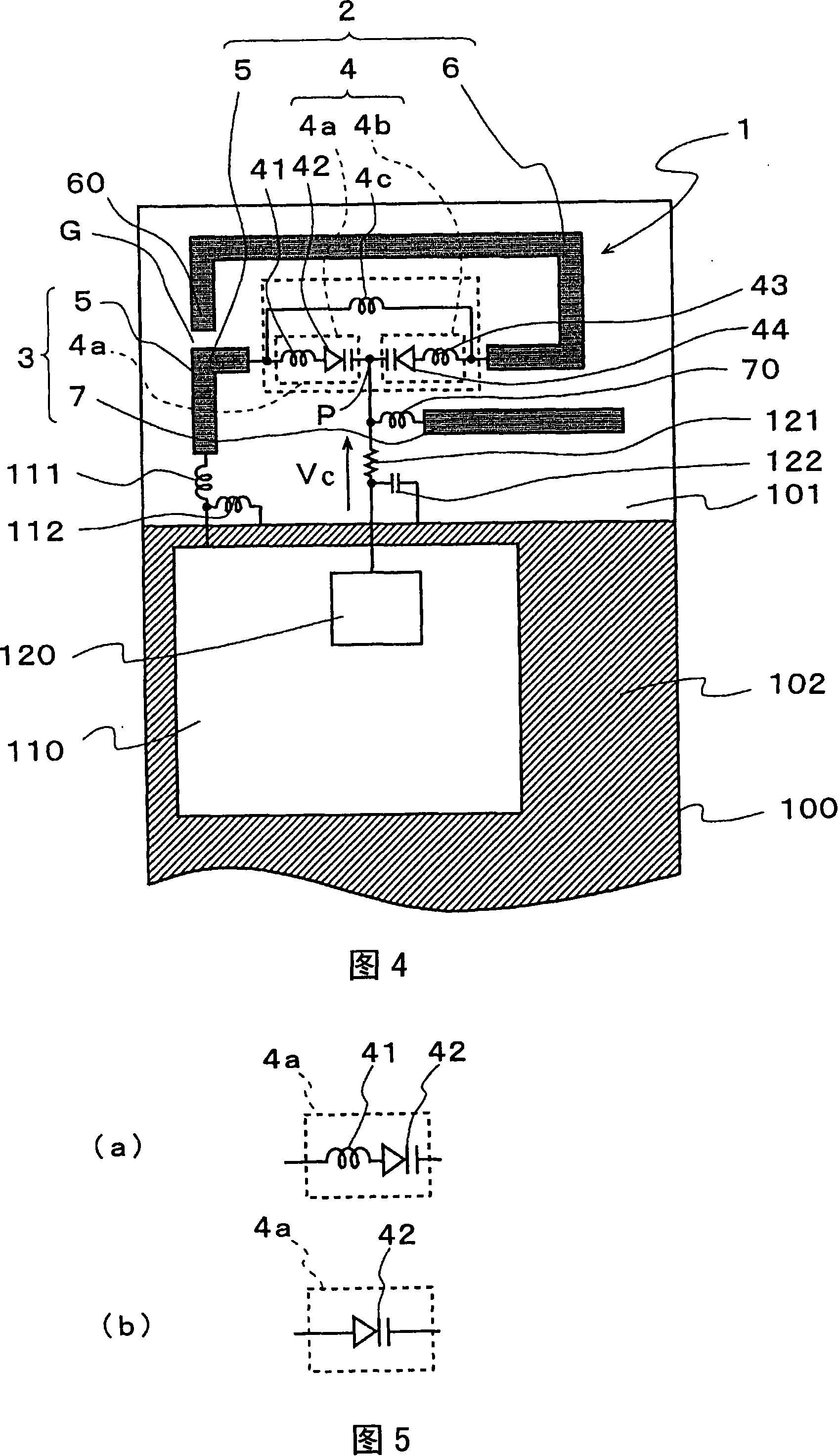
[0103] 4 is a schematic plan view showing an antenna according to a second embodiment of the present invention, FIG. 5 is a circuit diagram showing a specific example of a first reactance circuit 4a of a series circuit, and FIG. 6 is a circuit diagram showing a variable second reactance circuit 4b. The circuit diagram of the specific example.

[0104] Compared with the first reactance circuit 4 a and the second reactance circuit 4 b of the first embodiment, the antenna 1 of this embodiment adopts a specific variable series circuit.

[0105] As the first reactance circuit 4a is a series circuit including a variable capacitance element or a parallel circuit including a variable capacitance element, but in this embodiment, a series circuit including a variable capacitance element is employed. Among them, the series circuits shown in FIGS. 5( a ) and ( b ) are mentioned as the series circuit including the variable capacitance element. In this example, the series circuit of Fig. 5...

Embodiment 3

[0111] Next, a third embodiment of the present invention will be described.

[0112] FIG. 7 is a schematic plan view showing an antenna according to a third embodiment of the present invention, and FIG. 8 is a circuit diagram showing a specific example of a fixed second reactance circuit 4b.

[0113] In the second embodiment described above, a series circuit including variable capacitance elements is used as the first reactance circuit 4a, and a series circuit including variable capacitance elements or a parallel circuit including variable capacitance elements is used as the second reactance circuit 4b. , but in this embodiment, a series circuit including a fixed capacitance element or a parallel circuit including a fixed capacitance element is used as the second reactance circuit 4b.

[0114] Among them, as a series circuit including a fixed capacitance element or a parallel circuit including a fixed capacitance element, circuits shown in FIGS. 8( a ) to ( e ) are exemplified...


PUM


Abstract

An antenna and a wireless communication device in which a plurality of resonant frequencies can be changed simultaneously by a desired range at a low voltage are provided. An antenna 1 includes a first antenna section 2 and a second antenna section 3. The first antenna section 2 is formed of a feeding electrode 5, a frequency-changing circuit 4, and a radiating electrode 6, and the second antenna section 3 is formed of the feeding electrode 5, a first reactance circuit 4a, and an additional radiating electrode 7. The frequency-changing circuit 4 has a circuit configuration in which the first reactance circuit 4a and the second reactance circuit 4b are connected. When a control voltage Vc is applied to a node P, the reactances of the first and second reactance circuits 4a and 4b change in accordance with the magnitude of the control voltage Vc, so that a resonant frequency f1 of the first antenna section 2 and a resonant frequency f2 of the second antenna section 3 change simultaneously.

Description

technical field [0001] The present invention relates to an antenna and a wireless communication device used in wireless communication. Background technique [0002] In recent years, in wireless communication devices such as mobile phones, multi-resonance and multi-frequency bands have been developed in order to realize broadband. Furthermore, antennas capable of broadband transmission and reception by controlling multiple resonance frequencies have also been studied. In addition, an antenna in which the frequency is variable to achieve wide band is also conceivable. [0003] Conventionally, such antennas are disclosed in Patent Document 1 to Patent Document 3, for example. [0004] The antenna disclosed in Patent Document 1 is an inverted-F antenna device. Specifically, the antenna elements are arranged in parallel on ground conductors, and at least one coupling element is arranged in parallel between these ground conductors and the antenna elements. Furthermore, the ant...

Claims


Application Information

Patent Timeline
Patent Type & Authority Applications(China)
IPC IPC(8): H01Q9/14H01Q21/30H01Q5/01H01Q5/10
CPCH01Q1/243H01Q9/0442H01Q21/30H01Q5/371
Inventor 石塚健一川端一也
Owner MURATA MFG CO LTD
Why Eureka
Try Eureka