
Method for grid connecting with SOI dynamic threshold transistor through anti-off schottky

A technology of transistor and body region, which is applied in the field of silicon-on-insulator dynamic threshold transistor structure where the gate body is connected through a reverse biased Schottky junction, which can solve the problems of incompatibility with ordinary transistors.

Inactive Publication Date: 2007-12-19
INST OF MICROELECTRONICS CHINESE ACAD OF SCI
View PDF0 Cites 13 Cited by
  • Summary
  • Abstract
  • Description
  • Claims
  • Application Information

AI Technical Summary

Problems solved by technology

[0005] Due to the limitation of the working voltage, the gate body directly connected to the dynamic threshold transistor cannot be compatible with ordinary transistors of the same generation technology

Method used

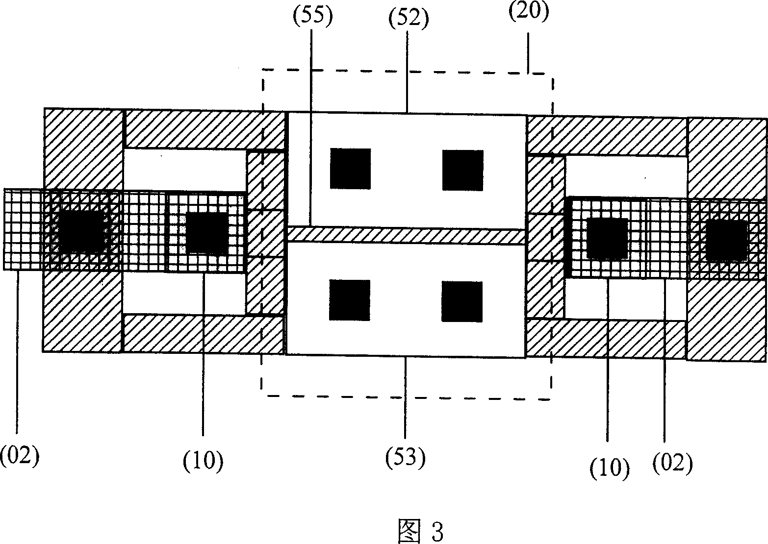

Image

  • Method for grid connecting with SOI dynamic threshold transistor through anti-off schottky
  • Method for grid connecting with SOI dynamic threshold transistor through anti-off schottky

Examples


Embodiment Construction

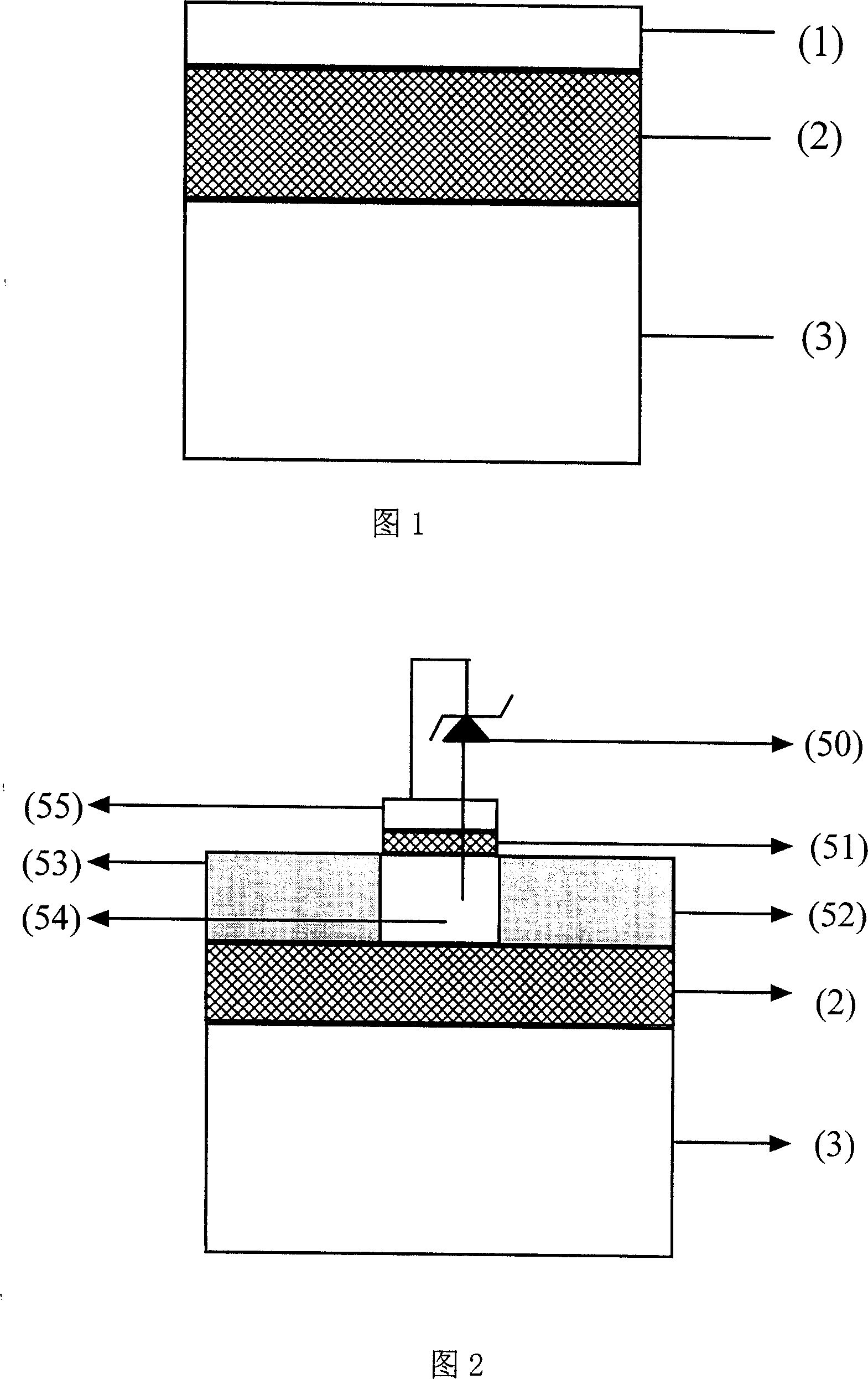
[0015] Figure 1 illustrates a starting SOI silicon wafer that can be used in the present invention. It contains an oxide buried layer (2) to electrically isolate the silicon substrate (3) from the top silicon film (1). A top silicon film (1), in which active device regions can be formed. The SOI silicon wafer can be fabricated by conventional SIMOX (Ion Implantation of Oxygen Ion Isolation) process known to those skilled in the art, or by other conventional processes including, for example, thermal bonding and dicing processes.

[0016] The present invention utilizes process steps compatible with conventional SOI CMOS processes. In order to electrically isolate the body regions of different devices from each other, isolation techniques such as MESA, STI or LOCOS can be used. When using STI and LOCOS isolation technology, the field oxygen should be in contact with the buried oxide layer.

[0017] Fig. 2 is a kind of structure of silicon-on-insulator dynamic threshold transis...


PUM


Abstract

This invention relates to a method that a grid is connected to a SOI dynamic threshold transistor by a pull-down Schottky joint including: a SOI substrate, a transistor formed in the SOI top layer silicom film and including a grid, a grid oxidation layer, a drain, a source and a transistor region and a pull-down Schottky joint connected between the grid and the transistor region, in which, a metal is used to connect the grid with a leading-out part of the transistor and necessary electric isolation should be done among appliances.

Description

technical field [0001] The invention relates to the technical field of semiconductor devices, in particular to a gate body connected to a silicon-on-insulator (SOI) dynamic threshold transistor structure through a reverse-biased Schottky junction and a related process method. Background technique [0002] The first SOI dynamic threshold transistor (DTMOS) structure, and also the first real DTMOS, was proposed by IBM Fariborz Assaderaghi et al. in 1994, which aroused widespread interest of researchers. The gate electrode of this device structure is directly connected to the body region, which is compatible with the traditional CMOS process and can effectively solve the contradiction between the operating voltage and the threshold voltage of nanoscale devices: in the off state, the device has a higher Threshold voltage, thereby reducing the leakage current; in the on-state condition, the device has a lower threshold voltage, thereby improving the driving ability. DTMOS reduce...

Claims


Application Information

Patent Timeline
Patent Type & Authority Applications(China)
IPC IPC(8): H01L27/12H01L29/78
Inventor 毕津顺海潮和韩郑生
Owner INST OF MICROELECTRONICS CHINESE ACAD OF SCI
Learn More