
System and method for accessing not-and flash memory

A flash memory and non-type technology, which is applied in the field of access and non-type flash memory systems, can solve the problems of only one chip in performance, reduce the access speed of the controller to NAND Flash, and it is difficult to meet the needs of high-performance and large-capacity equipment, so as to improve access The effect of speed and shortening the access delay

Active Publication Date: 2007-10-31
HUAWEI TECH CO LTD
View PDF0 Cites 15 Cited by
  • Summary
  • Abstract
  • Description
  • Claims
  • Application Information

AI Technical Summary

Problems solved by technology

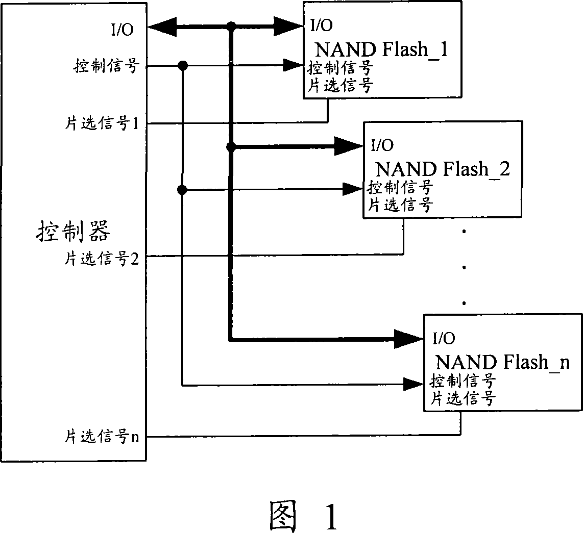
Although the structure of the existing method is relatively simple, the controller is also relatively easy to implement, but because the controller adopts the sequential access mode to the multi-chip NAND Flash connected to itself, when the storage capacity is required to be as large as possible, the control is seriously reduced. The access speed of the controller to NAND Flash, that is to say, no matter whether the controller is connected to a single-chip or multiple NAND Flash, the performance is only the performance of a single chip, which makes it difficult to meet the needs of high-performance and large-capacity equipment

Method used


Image

  • System and method for accessing not-and flash memory
  • System and method for accessing not-and flash memory
  • System and method for accessing not-and flash memory

Examples


Embodiment Construction

[0023] In order to make the object, technical solution and advantages of the present invention clearer, the present invention will be further described in detail below with reference to the accompanying drawings and preferred embodiments.

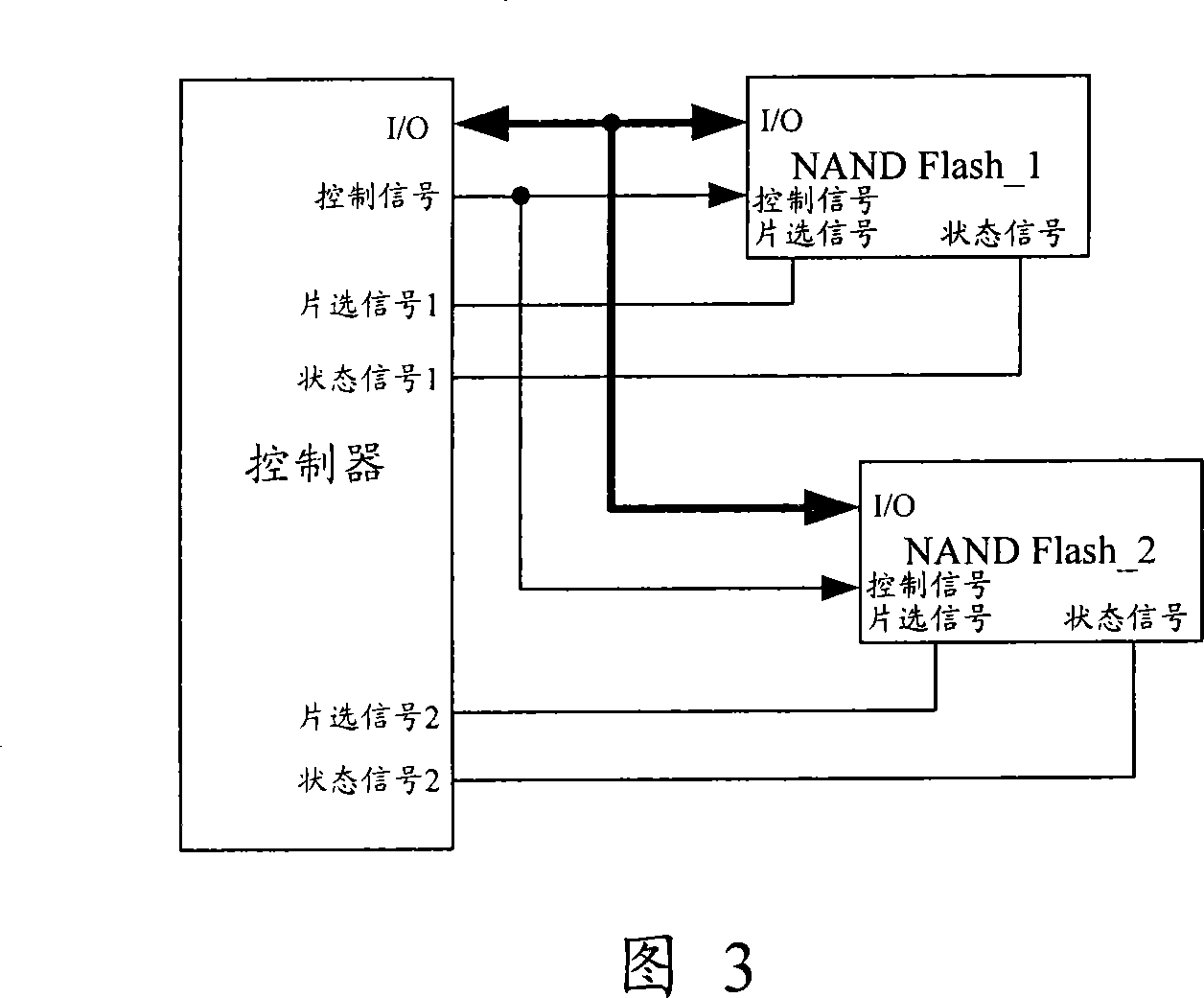
[0024] Fig. 3 is the embodiment one schematic diagram of the system topology structure of NAND Flash operation of the present invention, as shown in Fig. 3, system of the present invention comprises controller and two NAND Flash, passes I / O data between each NAND Flash and controller The signal, control signal, status signal and chip selection signal are connected. The I / O data signal and control signal of each piece of NAND Flash are shared, while the status signal and chip selection signal of each piece of NAND Flash are independent. Figure 3 includes a controller and two pieces of NAND Flash, where NAND Flash_1 and NAND Flash_2 are connected to the controller through shared I / O signals and control signals, and NAND Flash_1 and NAND Flash_...


PUM


Abstract

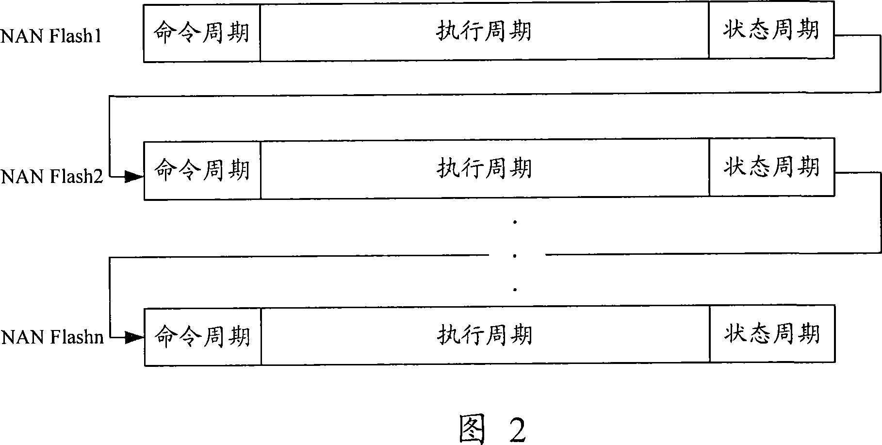
This invention discloses one visit and non-flash memory system and method, which comprises the following steps: through test on the memory operation and in the execution circle the controller sends operation orders to other memory chips to overlap the memory execution circles to realize the multiple memory operations and to reduce the visit time lag of controller and non-flash memory visit time lag.

Description

technical field [0001] The invention relates to flash memory technology, in particular to a system and method for accessing NAND Flash. Background technique [0002] Access to NAND Flash usually includes three cycles: command cycle, execution cycle and status cycle. In the command cycle, NAND Flash receives the execution command from the controller; in the execution cycle, NAND flash executes the command received; in the status cycle, the controller reads the result of the command execution from NAND Flash. [0003] The basic operations on NAND Flash include read operation, erase operation and programming operation. The operation process is respectively: [0004] When performing a read operation, the controller sends a read command to the NAND Flash during the command cycle, and the NAND Flash reads the page to be read during the execution cycle, and the controller can read data from the NAND Flash during the status cycle; when performing an erase operation, the controller...

Claims


Application Information

Patent Timeline
IPC IPC(8): G11C16/06
Inventor 麦嘉源
Owner HUAWEI TECH CO LTD
Learn More