Method of manufacturing wiring substrate
A technology for a wiring substrate and a manufacturing method, which is applied in the manufacture of printed circuits, resists for applying catalysts, liquid chemical plating, etc., can solve problems such as difficulty in fine wiring patterns, and achieve the effect of improving reliability.
- Summary
- Abstract
- Description
- Claims
- Application Information
AI Technical Summary
Problems solved by technology
Method used
Image
Examples
no. 1 example
[0033] First, the first embodiment will be described.
[0034] 1.1 Manufacturing method of wiring board
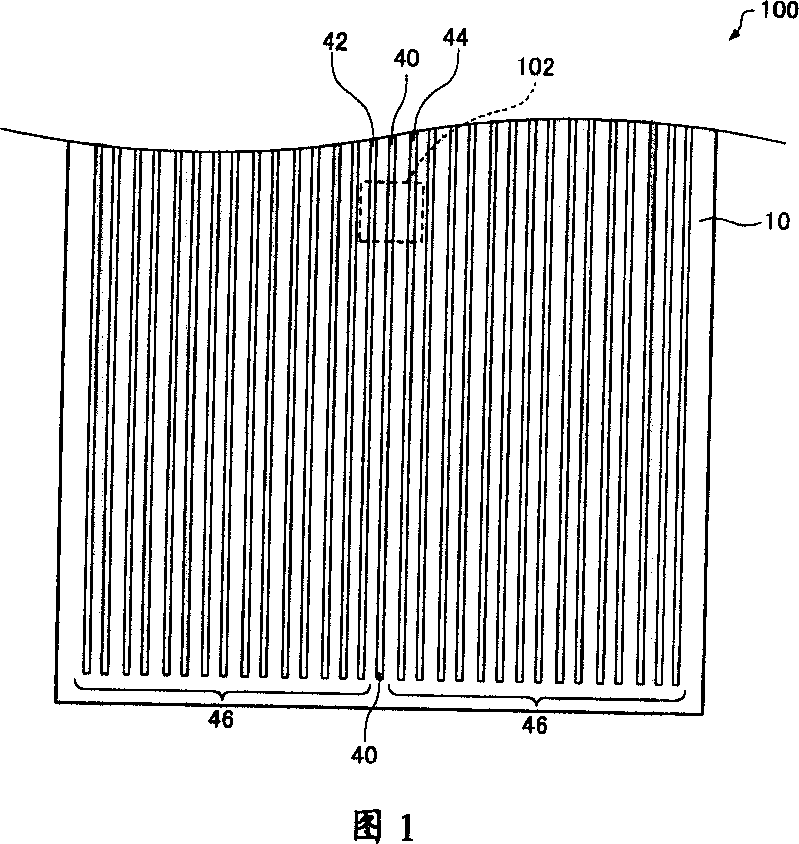
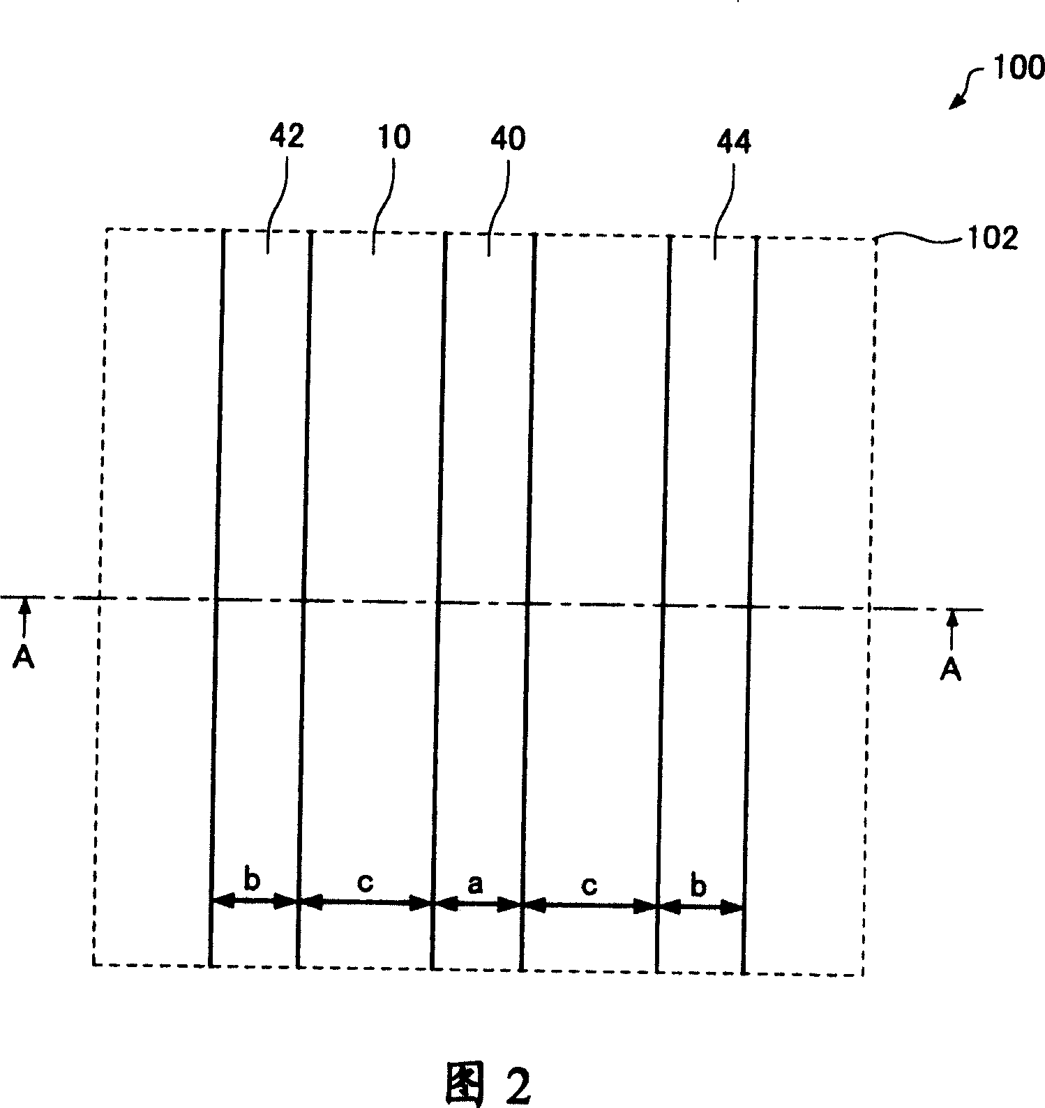
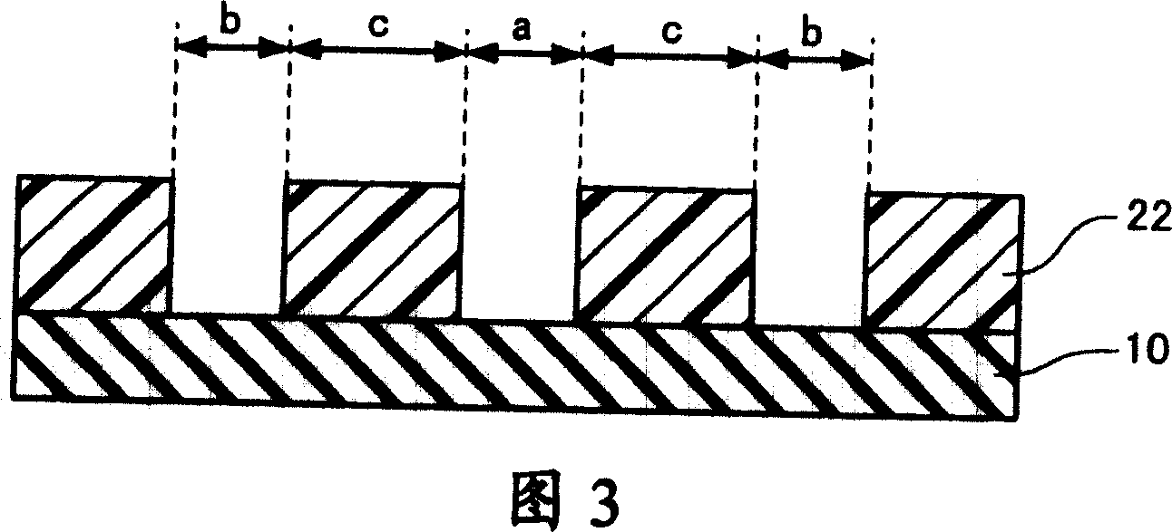
[0035] 1 to 10 are schematic diagrams showing an example of a method of manufacturing wiring board 100 (see FIG. 10 ) according to the first embodiment. 1 and 2 are plan views showing an example of a method of manufacturing a wiring board according to the first embodiment. FIG. 2 is an enlarged view of area 102 in FIG. 1 . 3 to 10 are cross-sectional views corresponding to the A-A cross-section of the wiring board in FIG. 2 .
[0036] (1) First, the substrate 10 is prepared. As shown in FIG. 3, the substrate 10 may be an insulating substrate. The substrate 10 may also be an organic substrate (such as plastic material, resin substrate), or an inorganic substrate (such as quartz glass, silicon wafer, oxide layer). Examples of the plastic material include polyimide, polyethylene terephthalate, polycarbonate, polyphenylene sulfide, and the like. Alternatively, the substr...
experiment example 2
[0065] (1) A photoresist film is formed on a glass substrate, and then, by direct writing, the photoresist film is exposed and developed in a linear form with a width of about 0.2 μm, thereby forming a photoresist layer, This photoresist layer has linear lines with a width of about 0.8 μm and a plurality of rows of line-shaped openings at intervals of about 0.2 μm. The total line width is about 16 μm.
[0066] (2) Next, the glass substrate was formed into a square of 1×1 cm, and immersed in a cationic surfactant solution (FPD Condeishyona manufactured by Technic Japan Co., Ltd., FPD conditioner manufactured by Technic Japan Co., Ltd.). Next, this glass substrate was immersed in a palladium catalyst solution. Then, the photoresist layer on the glass substrate is removed using an organic solvent such as acetone. Thus, a linear catalyst layer having linear lines with a width of about 0.8 μm and a space of about 0.2 μm was formed.
[0067] (3) Next, immerse the glass substrate ...
experiment example 3
[0083] By the method of manufacturing a wiring board according to the second embodiment, a pad-shaped metal layer was formed, and an experiment was performed to measure the film thickness. 15 is a graph showing the thickness of the metal layer relative to the pad width (one side of the square) of the catalyst layer. A specific method for forming the metal layer is as follows.
[0084] (1) Form a photoresist film on a glass substrate, and then, by direct writing, expose and develop the photoresist film in the form of a pad shape with a width of about 1 to 100 μm, thereby forming a film having a thickness of about 1 to 100 μm A photoresist layer for pad-shaped openings with a width of 100 μm.
[0085] (2) Next, the glass substrate was cut into a square of 1×1 cm, and immersed in a cationic surfactant solution (FPD Condeishyona, manufactured by Technic Japan Co., Ltd., FPD conditioner manufactured by Technic Japan Co., Ltd.). Next, this glass substrate was immersed in a palladi...
PUM
| Property | Measurement | Unit |
|---|---|---|
| thickness | aaaaa | aaaaa |
| width | aaaaa | aaaaa |
| width | aaaaa | aaaaa |
Abstract
Description
Claims
Application Information
 - Generate Ideas
- Intellectual Property
- Life Sciences
- Materials
- Tech Scout
- Unparalleled Data Quality
- Higher Quality Content
- 60% Fewer Hallucinations
Browse by: Latest US Patents, China's latest patents, Technical Efficacy Thesaurus, Application Domain, Technology Topic, Popular Technical Reports.
© 2025 PatSnap. All rights reserved.Legal|Privacy policy|Modern Slavery Act Transparency Statement|Sitemap|About US| Contact US: help@patsnap.com


