Manufacturing method of semiconductor package

一种制造方法、半导体的技术,应用在半导体/固态器件制造、半导体器件、半导体/固态器件零部件等方向,能够解决难以谋求作业性的提高、半导体芯片裂纹不良、贯通电极电极材料填充困难等问题,达到提高操作和作业性的效果

Active Publication Date: 2007-08-15
TAIWAN SEMICON MFG CO LTD
View PDF1 Cites 6 Cited by
  • Summary
  • Abstract
  • Description
  • Claims
  • Application Information

AI Technical Summary

Problems solved by technology

[0005] However, according to the above-mentioned conventional manufacturing method, it is difficult to handle the thinned intervening sheet divided into individual pieces, and it is difficult to improve workability.
As a result, defects such as cracks are likely to occur in the semiconductor chip, which may lower the yield
Therefore, it is conceivable to improve handling performance by increasing the thickness of the intervening sheet, but there is a disadvantage that not only the overall thickness of the package increases, but also the formation of through electrodes or the filling of electrode materials becomes significantly difficult.

Method used


Image

  • Manufacturing method of semiconductor package
  • Manufacturing method of semiconductor package
  • Manufacturing method of semiconductor package

Examples


Embodiment Construction

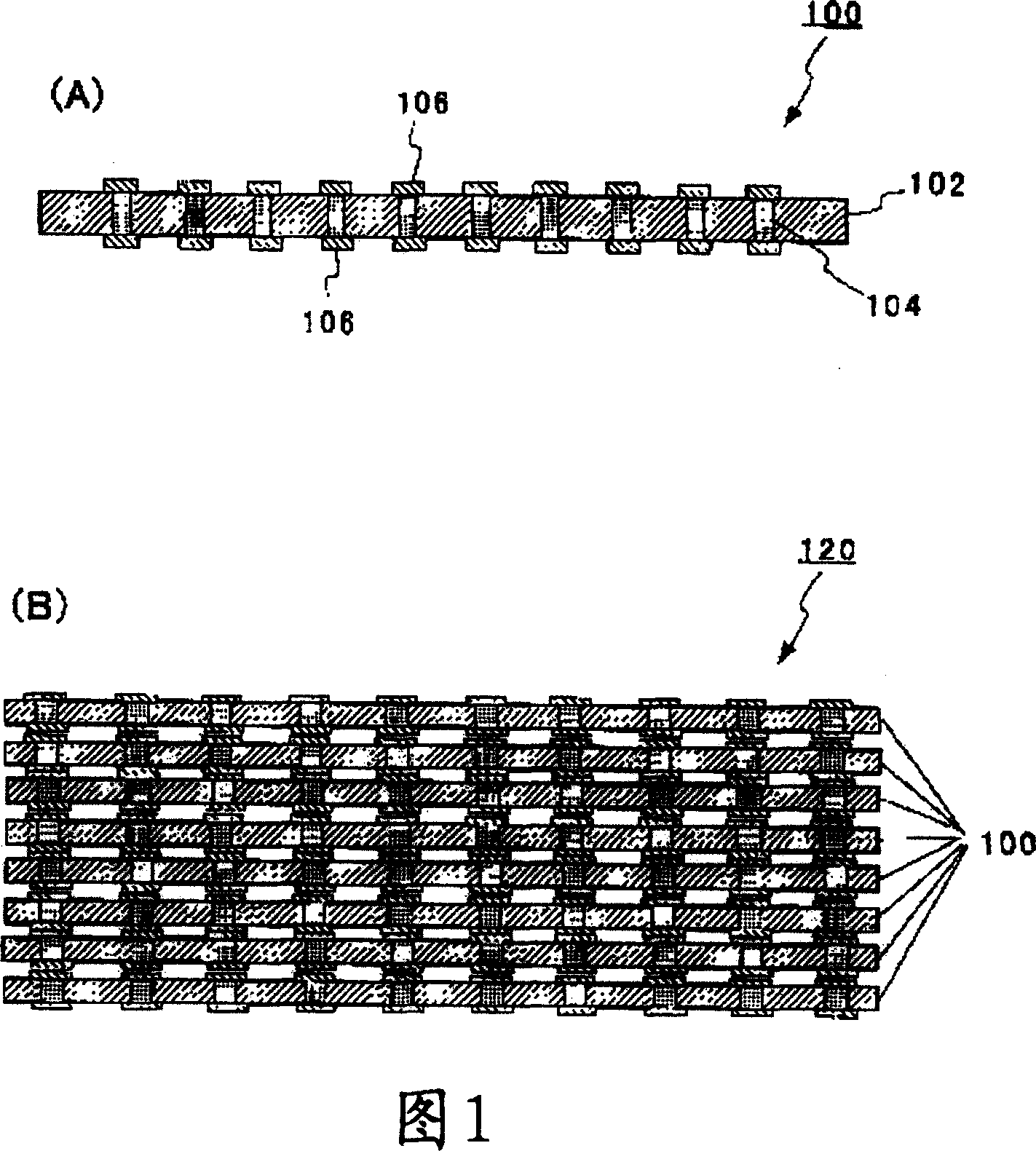
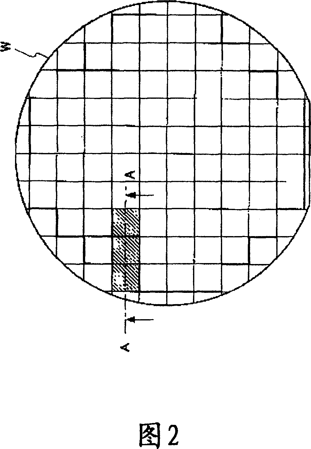
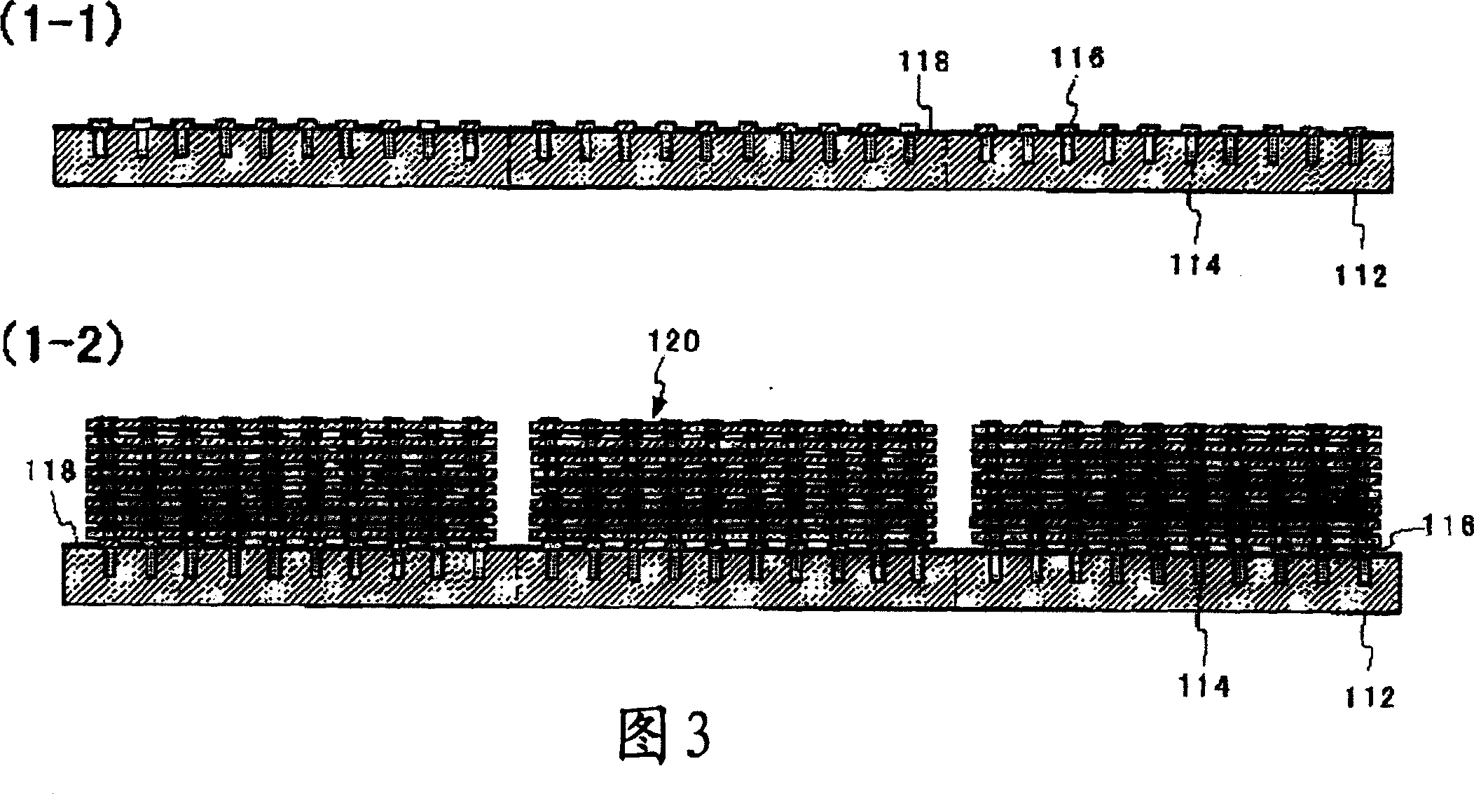
[0028] Hereinafter, the best mode for carrying out the present invention will be described in detail using examples. FIG. 1 is a schematic cross-sectional view showing the structure of a semiconductor chip (A) and its laminate (B) applicable to a semiconductor package according to the present invention. 2 is a schematic plan view showing a silicon wafer for an interposer applicable to the semiconductor package of the present invention. The semiconductor chip 100 has a structure in which bumps 106 are formed on both surfaces of the front and rear surfaces of the semiconductor substrate 102 on which the penetrating electrodes 104 are provided. In addition, a structure in which the bump 106 is formed only on one side of the semiconductor substrate 102 may also be used. The thickness of the semiconductor substrate 102 is desirably 20 to 100 μm from the depth of the through-electrodes. For convenience of description, it is assumed that the structure in which the semiconductor chi...


PUM


Abstract

The invention provides a method for fabricating semiconductor package which can improve the performance. According to this invention, a method for fabricating a semiconductor package, comprising: mounting and layering a plurality of semiconductor chips on a first surface of a semiconductor wafer, which is to be used for a semiconductor interposer; forming a mold resin over the semiconductor chips to cover the semiconductor chips entirely; and dicing the semiconductor wafer to form a plurality of individual semiconductor packages.

Description

technical field [0001] The present invention relates to a method of manufacturing a semiconductor package in which a plurality of semiconductor chips are stacked on an interposer sheet having through electrodes. Background technique [0002] In recent years, the "system in package" (System in Package) technology that mounts a plurality of semiconductor chips of an integrated circuit at a high density and realizes a high-function system in a short period of time has attracted more and more attention. In particular, there is an increasing demand for a stacked package that can achieve significant miniaturization by stacking a plurality of semiconductor chips three-dimensionally. As a technology that meets such demands, for example, as disclosed in JP-A-2005-236245 , it has been proposed to form a through-hole electrode inside a semiconductor chip and laminate it on a chip for mounting called an interposer. Semiconductor package structure. [0003] [Patent Document 1] JP-A-200...

Claims


Application Information

Patent Timeline
Patent Type & Authority Applications(China)
IPC IPC(8): H01L21/50
CPCH01L25/50H01L2224/73203H01L23/3135H01L2924/01047H01L2924/01079H01L2224/97H01L25/0657H01L2924/14H01L24/97H01L2924/01033H01L2225/06513H01L2924/01005H01L2924/15311H01L2225/06541H01L2924/01006H01L2924/01029H01L2924/01074H01L21/563H01L2924/01013H01L21/561H01L2924/181H01L2224/81H01L2924/00H01L23/28H01L23/04
Inventor 江川良实
Owner TAIWAN SEMICON MFG CO LTD
Why Eureka
Try Eureka