Variegated BIST test approach

A test method and test pattern technology, applied in the direction of digital circuit test, electronic circuit test, measurement of electricity, etc., can solve the problems of large area and increase of test time, and achieve the effect of increasing test depth, increasing test ability and reducing dependence.

Active Publication Date: 2010-02-17
SHANGHAI HUAHONG GRACE SEMICON MFG CORP
View PDF6 Cites 0 Cited by
  • Summary
  • Abstract
  • Description
  • Claims
  • Application Information

AI Technical Summary

Problems solved by technology

[0007] In order to solve the problem of too large area and increase the number of simultaneous measurements, some SOC designs add serial port circuits to pass all excitation signals through very few PADs (pins) such as figure 1 There are only PAD1 and PAD2 in the middle, so to take into account all the test error coverage, the depth of the excitation signal is bound to increase a lot, the test time increases, and the ability of the hardware graphics of the tester is challenged

Method used


Image

  • Variegated BIST test approach
  • Variegated BIST test approach

Examples


Embodiment Construction

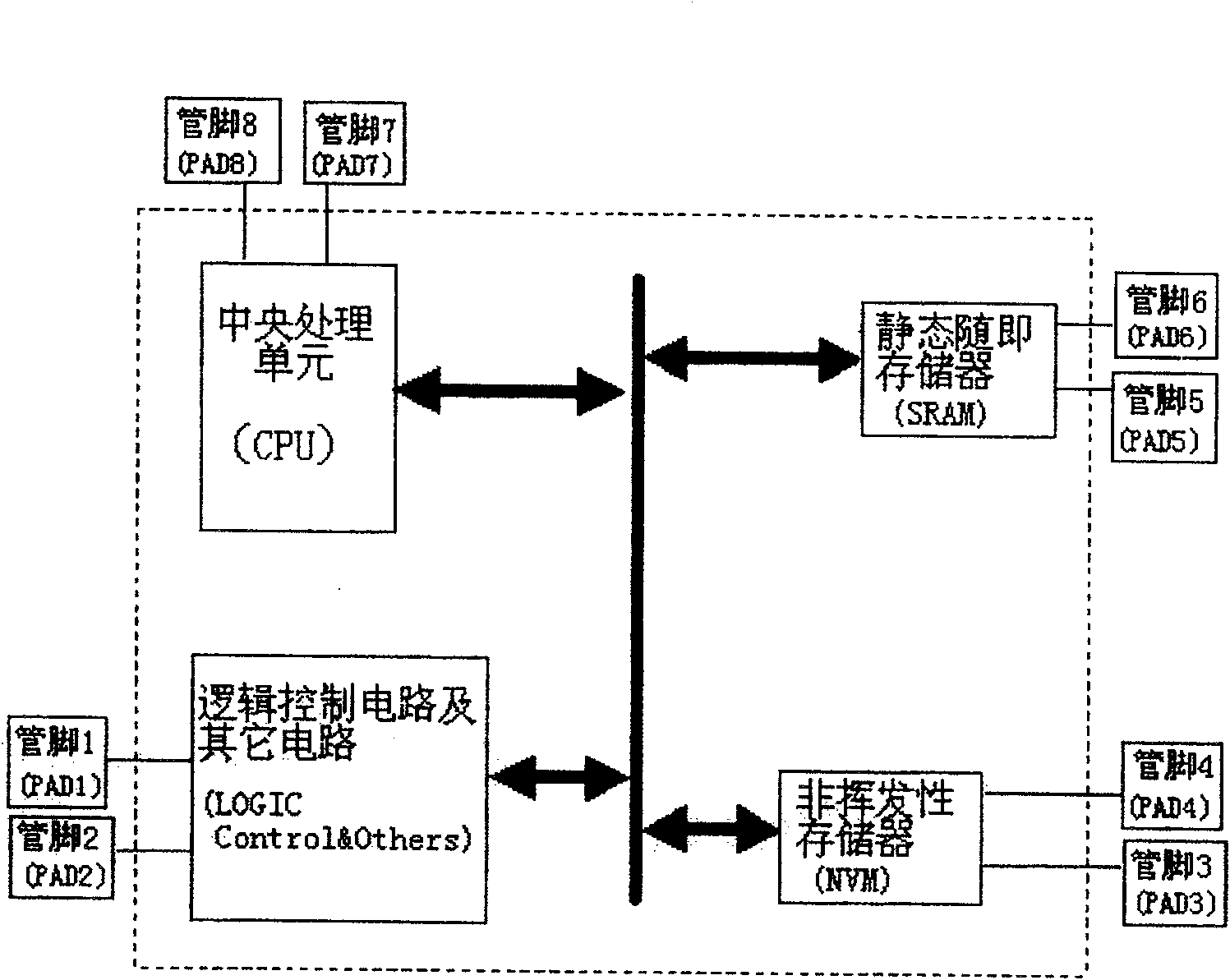
[0019] The BIST test method of the present invention utilizes some resources of the chip itself, especially the rewritable memory resources, to test other part functions of the chip, so as to reduce the impact on the test platform and the chip itself on the basis of ensuring the test error coverage rate. design requirements.

[0020] The embedded Flash area of ​​the chip is usually used to store software codes in actual product applications, and is used for the instruction library for its CPU to operate the system. Use this feature to store all the functional instructions to be tested in the NVM (Non-Volatile Memory, non-volatile memory) area in advance, and then activate the CPU through simple external instructions to call and operate these instructions in the storage area. .

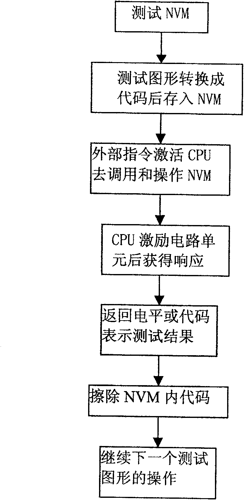
[0021] The BIST test method of the present invention comprises reducing the number of pins, and also includes the following steps (see figure 2 ):

[0022] (1) Test the NVM through the logical inte...


PUM


Abstract

The invention relates to a method for chip testing and discloses a diversified test method for BIST, which comprises the following steps: test the NVM through the logic Interface unit; convert the test image to the instruction set in the code form and store in the NVM area; the CPU enabled by the external instructions reads the instruction set in the NVM area and energizes the circuit in the chipaccording to the instruction set; after receiving the response, return the PWL or code on the inport or output; erase the code in the NVM, repeat the above steps and then conduct operation of the nexttest image. The diversified test method for BIST provided in the invention can greatly save the chip area and test channel, increase the concurrent-testing capacity and reduce the dependence to the test hardware.

Description

technical field [0001] The invention relates to a chip testing method, in particular to a BIST (Built In Self Test, built-in self-test) testing method. Background technique [0002] During the chip test, the tester is used to apply excitation to the chip from the outside, and then the response is compared with the expectation to judge whether the chip is a good product. [0003] More complex chips need more pins, lead out the channels required for testing and connect them with the testing channels, one-to-one correspondence, receive the excitation of the tester, and return the signal to the tester for judgment, but this method The chip area is too large and the cost is too high. [0004] In order to save the chip area, some designs will reduce the PAD of the chip and reduce the test channels. In order to achieve the same error coverage, the depth of the test pattern will inevitably be deepened. However, existing testers or some test software may not be able to meet these r...

Claims


Application Information

Patent Timeline
Patent Type & Authority Patents(China)
IPC IPC(8): G01R31/28G01R31/317G01R31/3187
Inventor 陈凯华谢晋春陈婷辛吉升桑浚之
Owner SHANGHAI HUAHONG GRACE SEMICON MFG CORP
Why Eureka
Try Eureka