TTL and CMOS compatible input buffer

An input buffer and input buffer technology, applied in the direction of logic circuit connection/interface layout, logic circuit coupling/interface using field effect transistors, etc. The effect of high consumption and high speed

Active Publication Date: 2009-12-30
BEIJING MXTRONICS CORP +1
View PDF3 Cites 0 Cited by
  • Summary
  • Abstract
  • Description
  • Claims
  • Application Information

AI Technical Summary

Problems solved by technology

But in practice, the flipping point set by this solution is easily changed by process and supply voltage changes

Method used


Image

  • TTL and CMOS compatible input buffer
  • TTL and CMOS compatible input buffer
  • TTL and CMOS compatible input buffer

Examples


Embodiment Construction

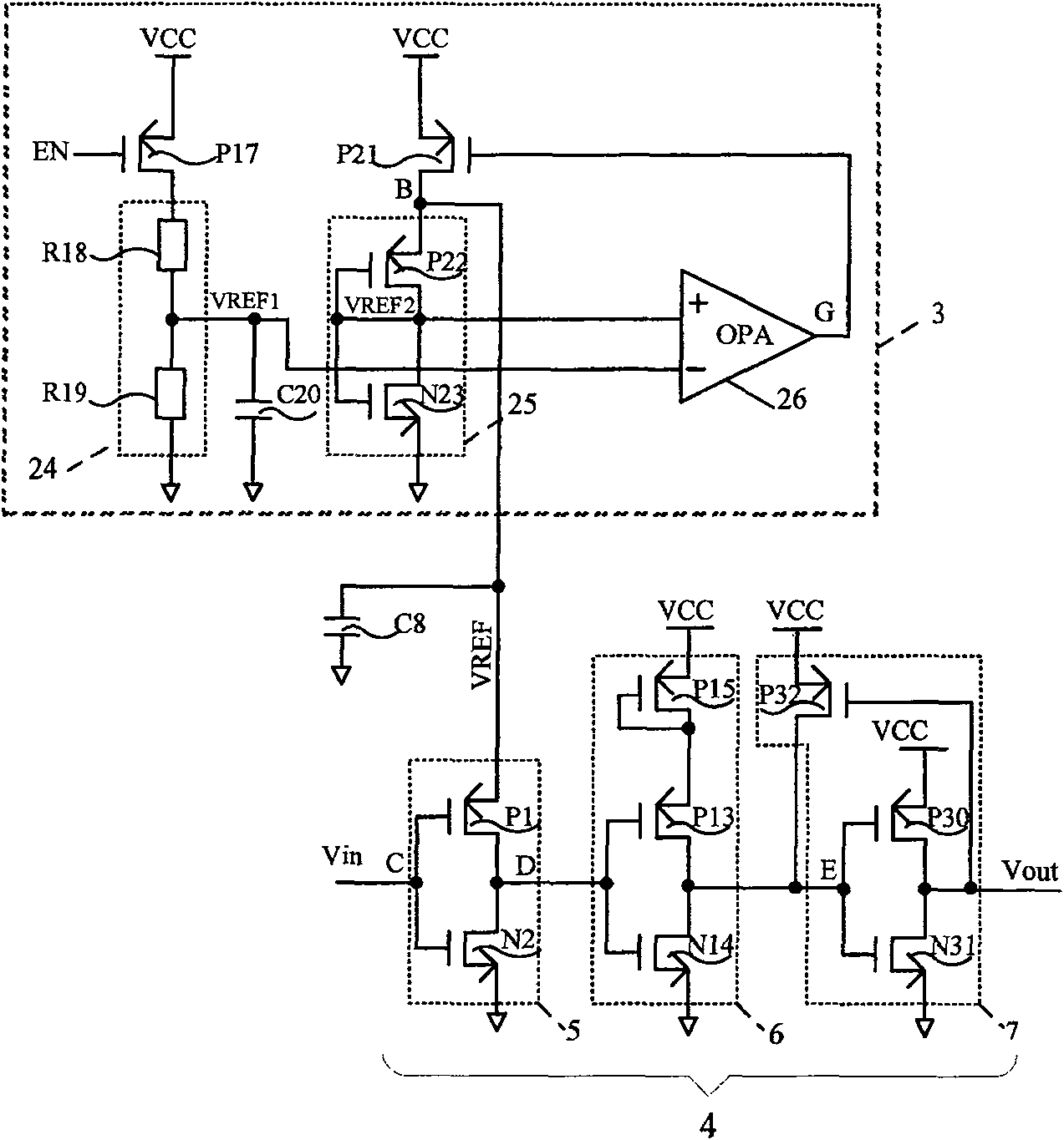
[0020] Such as figure 1 Shown is the schematic block diagram of the circuit of the TTL and CMOS compatible input buffer of the present invention, including a reference voltage generator 3 and an input buffer 4, and the reference voltage generator 3 includes a resistor divider network 24, a reference input buffer 25 and an operation The amplifier 26 and the input buffer 4 include an input inverter 5 , a second-stage input inverter 6 and a third-stage input inverter 7 .

[0021] The MOS transistors used in the present invention are all enhanced devices.

[0022] The input inverter 5 in the input buffer 4 is composed of a PMOS transistor P1 and an NMOS transistor N2, and the gate of the PMOS transistor P1 is connected to the gate of the NMOS transistor N2 as the input terminal of the input inverter 5, and the gate of the PMOS transistor P1 The drain is connected to the drain of the NMOS transistor N2 as the output of the input inverter 5 , the source of the NMOS transistor N2 is...


PUM


Abstract

A TTL and CMOS compatible type input buffer comprises a reference voltage generator and an input buffer which comprises at least one stage input invertor which include a PMOS tube P1 and an NMOS tube N2, the grids of which are connected as an input end for inputting signal Vin, a source pole of the PMOS tube P1 is connected with a reference voltage VREF provided by the reference voltage generator; when the circuit works in the TTL mode, the reference voltage generator provides reference voltage VREF for the input invertor between 3.3 and 3.5 V, the turning point voltage of the input invertor is 1.4 V to make input noise margin maximum; when the circuit works in the CMOS mode, the reference voltage generator has no quiescent power dissipation, the reference voltage generator provides reference voltage VREF for the input invertor between 4.6 and 5 V, the turning point voltage of the input invertor is 2.5 V to obtain the maximum noise margin.

Description

technical field [0001] The invention relates to an input buffer, in particular to a TTL and CMOS compatible input buffer. Background technique [0002] Bipolar ICs operate in low voltage logic. Usually the logic 0 of the TTL logic circuit is between 0.0-0.8V, and the logic 1 is between 2.0-5.0V. Therefore, to be able to distinguish between 0 and 1, a CMOS inverter operating in TTL mode must be able to flip at some point between 0.8V and 2.0V, preferably close to 1.4V, in order to provide maximum noise margin. The CMOS inverter usually works at 4.5-15V, and the typical value is 5V. In this way, if the source of the PMOS transistor in the CMOS inverter is connected to a 5V power supply voltage VCC, and its gate is connected to TTL logic 1 (2V), the PMOS transistor cannot be effectively cut off, and the PMOS transistor and the NMOS transistor are in simultaneous conduction. On-state, resulting in static short-circuit current, increasing the power consumption of the circuit. ...

Claims


Application Information

Patent Timeline
Patent Type & Authority Patents(China)
IPC IPC(8): H03K19/0175H03K19/0185
Inventor 陈雷林彦君文治平储鹏王勇李学武周涛张彦龙刘增荣尚祖宾
Owner BEIJING MXTRONICS CORP
Why Eureka
Try Eureka