False proof structure used for card and certificate and its identifying method
An identification method and card technology, applied in the field of card anti-counterfeiting technology and public safety, can solve the problems of high anti-counterfeiting cost, long detection time, and inappropriateness
- Summary
- Abstract
- Description
- Claims
- Application Information
AI Technical Summary
Problems solved by technology
Method used
Image
Examples
Embodiment 1
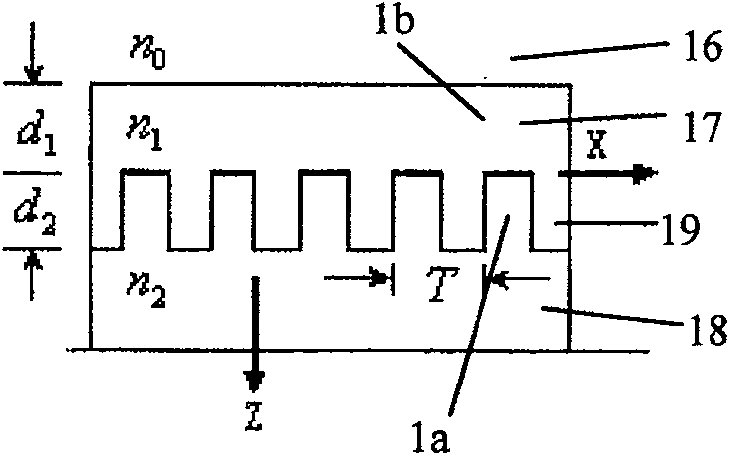
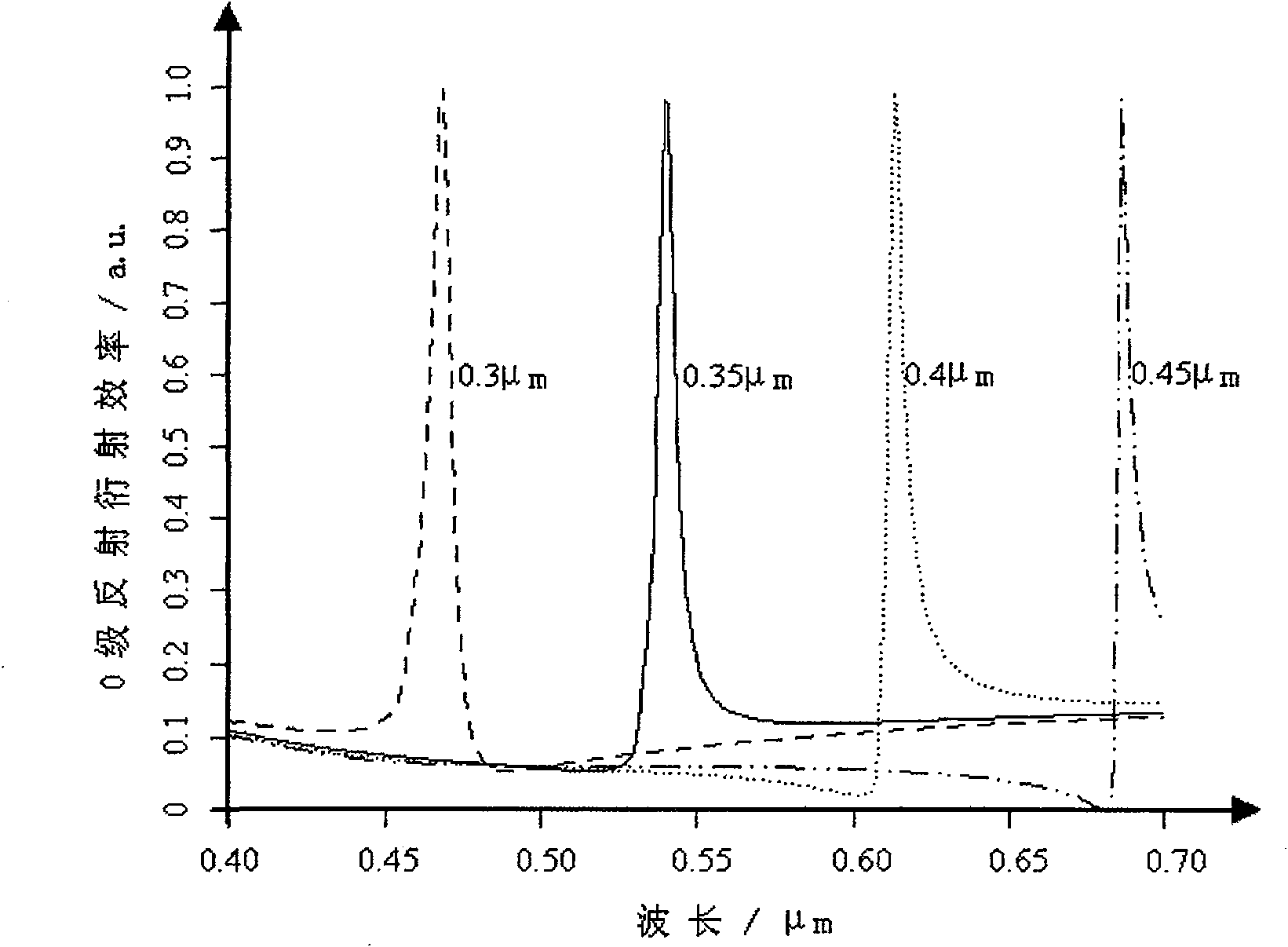
[0064] Embodiment 1: An anti-counterfeit structure for a card. On the body of the card to be anti-counterfeited, an identification pattern composed of a grating structure is provided. The identification pattern includes at least two types of graphic areas, and the two types of graphic areas are The orientation of the grating structure is arranged orthogonally to form a dual visual channel, and the two graphic areas do not overlap each other; the grating period of the grating structure is 300-500 nanometers, the groove depth is 50-150 nanometers, and the grating structure is filled with A transparent high-refractive index medium layer, the thickness of the medium layer is 20-30 nanometers, and the refractive index of the medium is greater than 1.6. The microstructure can be made by electron beam or laser beam lithography technology, and the high refractive index medium can be made by vacuum coating technology.
[0065] See attached Figure 7a , the image is a schematic diagram...
Embodiment 2
[0066] Embodiment 2: An anti-counterfeiting structure for a card. On the body of the card to be anti-counterfeited, an identification pattern composed of a grating structure is provided. The identification pattern includes at least two types of graphic areas, and the two types of graphic areas are The orientation of the grating structure is arranged orthogonally to form a dual visual channel, and the two graphic areas do not overlap each other; the grating period of the grating structure is 300-500 nanometers, the groove depth is 50-150 nanometers, and the grating structure is filled with A transparent high-refractive index medium layer, the thickness of the medium layer is 20-30 nanometers, and the refractive index of the medium is greater than 1.6. There is a third graphic area, which is composed of microstructured graphics with directional scattering characteristics. The line width of the grating structure that constitutes the microstructured graphics varies randomly within ...
PUM
 Abstract
Description
Claims
Application Information
 - R&D
- Intellectual Property
- Life Sciences
- Materials
- Tech Scout
- Unparalleled Data Quality
- Higher Quality Content
- 60% Fewer Hallucinations
Browse by: Latest US Patents, China's latest patents, Technical Efficacy Thesaurus, Application Domain, Technology Topic, Popular Technical Reports.
© 2025 PatSnap. All rights reserved.Legal|Privacy policy|Modern Slavery Act Transparency Statement|Sitemap|About US| Contact US: help@patsnap.com


