Packaging structure
A packaging structure and carrier technology, applied in electrical components, electrical solid devices, circuits, etc., can solve problems such as poor heat dissipation
- Summary
- Abstract
- Description
- Claims
- Application Information
AI Technical Summary
Problems solved by technology
Method used
Image
Examples
no. 1 example
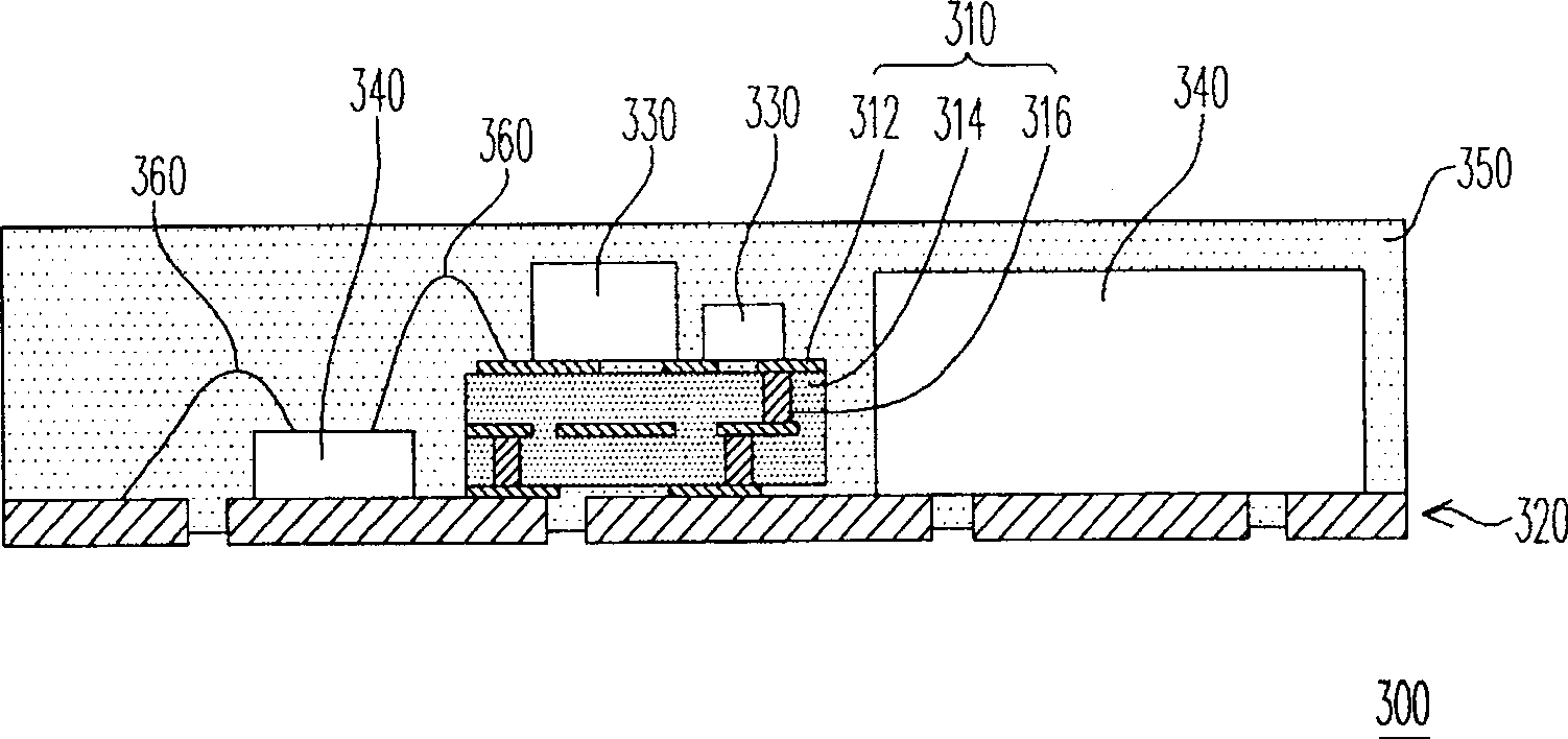
[0050] see image 3 , which shows a schematic cross-sectional view of the packaging structure of the first embodiment of the present invention. The packaging structure 300 of the first embodiment includes a first carrier 310, a second carrier 320, at least one first electronic component 330 ( image 3 For example, two) and at least one second electronic component 340 ( image 3 For example, two are shown). The second carrier 320 is electrically connected to the first carrier 310 , and the thermal resistance of the first carrier 310 may be greater than the thermal resistance of the second carrier 320 . The first electronic components 330 are disposed on the first carrier 310 and electrically connected to the first carrier 310 . The second electronic components 340 are disposed on the second carrier 320 and electrically connected to the second carrier 320 , and the heating power of each first electronic component 330 may be smaller than that of each second electronic componen...
no. 2 example
[0056] see image 3 and Figure 4 shown, where Figure 4 A schematic cross-sectional view of a packaging structure according to a second embodiment of the present invention is shown. The main difference between the packaging structure 400 of the second embodiment and the packaging structure 300 of the first embodiment is that the first electronic components 430 can be disposed on the opposite surfaces 412 , 414 of the first carrier 410 . In the second embodiment, the first carrier 410 can still be configured on the second carrier 420 . The second carrier 420 has a first carrying area 422 and a second carrying area 424 , and the first carrying area 422 and the second carrying area 424 are not on the same plane. In other words, just Figure 4 In terms of the relative positions shown, there is a height difference H between the second carrying area 424 and the first carrying area 422 . In addition, the first carrier 410 is disposed on the first carrying area 422 , and the sec...
no. 3 example
[0059] see image 3 , Figure 4 and Figure 5 shown, where Figure 5 A schematic cross-sectional view of a package structure according to a third embodiment of the present invention is shown. The main difference between the packaging structure 500 of the third embodiment and the packaging structures 300 and 400 of the above-mentioned embodiments is that the first carrier 510 of the third embodiment can be arranged beside the second carrier 520 . In addition, the package structure 500 further includes at least one bonding wire 560 ( Figure 5 Three lines are shown), the first carrier 510 is electrically connected to the second carrier 520 through at least one of the bonding wires 560 . In addition, the first carrier 510 may have a plurality of solder pads 516 disposed on a surface 514 of the first carrier 510 and exposed to the glue 550 . Compared with the above-mentioned embodiments, the solder pads 516 exposed from the glue 550 in the third embodiment can transmit electr...
PUM
 Abstract
Description
Claims
Application Information
 - R&D Engineer
- R&D Manager
- IP Professional
- Industry Leading Data Capabilities
- Powerful AI technology
- Patent DNA Extraction
Browse by: Latest US Patents, China's latest patents, Technical Efficacy Thesaurus, Application Domain, Technology Topic, Popular Technical Reports.
© 2024 PatSnap. All rights reserved.Legal|Privacy policy|Modern Slavery Act Transparency Statement|Sitemap|About US| Contact US: help@patsnap.com


