Method for using special chelant for micro electronic

A chelating agent and microelectronics technology, applied in the field of microelectronics, can solve the problem that the content of metal ions cannot be effectively reduced

Inactive Publication Date: 2008-10-01
HEBEI UNIV OF TECH
View PDF8 Cites 0 Cited by
  • Summary
  • Abstract
  • Description
  • Claims
  • Application Information

AI Technical Summary

Problems solved by technology

[0007] (4) only suitable for alkaline solution
Because the chelating agent complexes with the metal ions on the surface of the wafer, and due to the reduction of silicon, a part of the metal ions are reduced to atoms and exist on the surface of the wafer, so that the effect of the chelating agent cannot be fully exerted, so the substrate surface After processing, its metal ion content cannot be effectively reduced

Method used


Image

  • Method for using special chelant for micro electronic

Examples


Embodiment 1

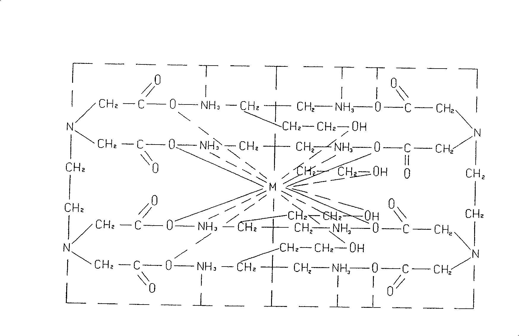
[0024] Put the abrasive sheet into the polishing machine, add 0.1% of the microelectronics special chelating agent diethylenediaminetetraacetic acid tetrahydroxyethylethylenediamine salt to the common polishing liquid by volume percentage, the polishing liquid is alkaline, and the pH value is 13, and then polish according to the conventional polishing method.

[0025] Then put the above-mentioned polishing sheet into the cleaning tank, add 0.1% of the microelectronics special chelating agent diethylenediaminetetraacetic acid tetrahydroxyethylethylenediamine salt, and 1% hydrogen peroxide as the oxidant in the cleaning agent, and then follow the routine cleaning method to obtain clean wafers.

Embodiment 2

[0027] Put the abrasive sheet into the polishing machine, the polishing liquid is acidic, the pH value is 1, and 3% of the microelectronics special chelating agent diethylenediaminetetraacetic acid tetrahydroxyethylethylenediamine salt is added to the above polishing liquid according to the volume percentage , and 1% hydrogen peroxide as the oxidant, and then polished according to the conventional polishing method.

[0028] Then put the above-mentioned polishing sheet into the cleaning tank, add 3% of the microelectronics special chelating agent diethylenediaminetetraacetic acid tetrahydroxyethylethylenediamine salt, and 3% hydrogen peroxide as the oxidant in the cleaning agent, and then follow the routine cleaning method to obtain clean wafers.

Embodiment 3

[0030] Put the abrasive sheet into the polishing machine, the polishing liquid is acidic, the pH value is 3, and 1% of the microelectronics special chelating agent diethylenediaminetetraacetic acid tetrahydroxyethylethylenediamine salt is added to the above polishing liquid according to the volume percentage , and 2% hydrogen peroxide as the oxidant, and then polished according to the conventional polishing method.

[0031] Then put the above-mentioned polishing sheet into the cleaning tank, add 1% of the microelectronics special chelating agent diethylenediaminetetraacetic acid tetrahydroxyethylethylenediamine salt, and 5% hydrogen peroxide as the oxidant in the cleaning agent, and then follow the conventional method. cleaning method to obtain clean wafers.


PUM


Abstract

The present invention provides micro-electronics special used chelating agent uses method for effectively removing metal ion on base material surface. It contains adding 0.1-3 per cent micro-electronics special chelating agent diethylenediamine tetraacetic acid tetrahydroxy ethyl ethylene diamine in usual polishing solution by volume, if polishing solution being basicity then polishing; if polishing solution being acidity then adding 1-5 per cent oxyful in above-mentioned polishing solution then polishing; putting above-mentioned polished section in purge tank and adding 0.1-3 per cent micro-electronics special chelating agent diethylenediamine tetraacetic acid tetrahydroxy ethyl ethylene diamine in cleaning agent by volume percentage, and 1-5 per cent oxyful, then to make cleaning. The present invention can oxidize metal atom existing chip surface to metal ion and fully chelating with chelating agent, thereby to obtain removing.

Description

technical field [0001] The invention relates to the field of microelectronics, and more particularly, to a special chelating agent for microelectronics, diethylenediaminetetraacetic acid tetrahydroxyethylethylenediamine salt, which can effectively remove metals in surface ultra-precision processing such as microelectronics polishing and cleaning. How to use ions. Background technique [0002] With the development of ultra-large-scale integrated circuits, the integration level continues to increase, the feature size of the device continues to decrease, and the requirements for the surface cleanliness of the silicon substrate are more stringent. The importance of silicon wafer cleaning in the semiconductor industry has long been paid attention to. , the VLSI process requires no more than 500 adsorbents / m on the provided substrate 2 ×0.12μm, metal pollution is less than 1010atom / cm 2 . Heavy metals (mainly from cutters) are called "deep level impurities" when their energy le...

Claims


Application Information

Patent Timeline
Patent Type & Authority Patents(China)
IPC IPC(8): H01L21/302H01L21/304H01L21/306C07D487/22
Inventor 刘玉岭李广福张西慧
Owner HEBEI UNIV OF TECH
Why Eureka
Try Eureka