Optical electronic apparatus and method for producing the same
A technology for optoelectronic devices and optoelectronic components, which is applied in the manufacture of optical heads, semiconductor/solid-state devices, circuits, etc., can solve the problems of difficulty in providing adhesives, inability to introduce and set nozzles, and generation of air bubbles, and achieve easy optical position alignment. Effect
- Summary
- Abstract
- Description
- Claims
- Application Information
AI Technical Summary
Problems solved by technology
Method used
Image
Examples
Embodiment 1
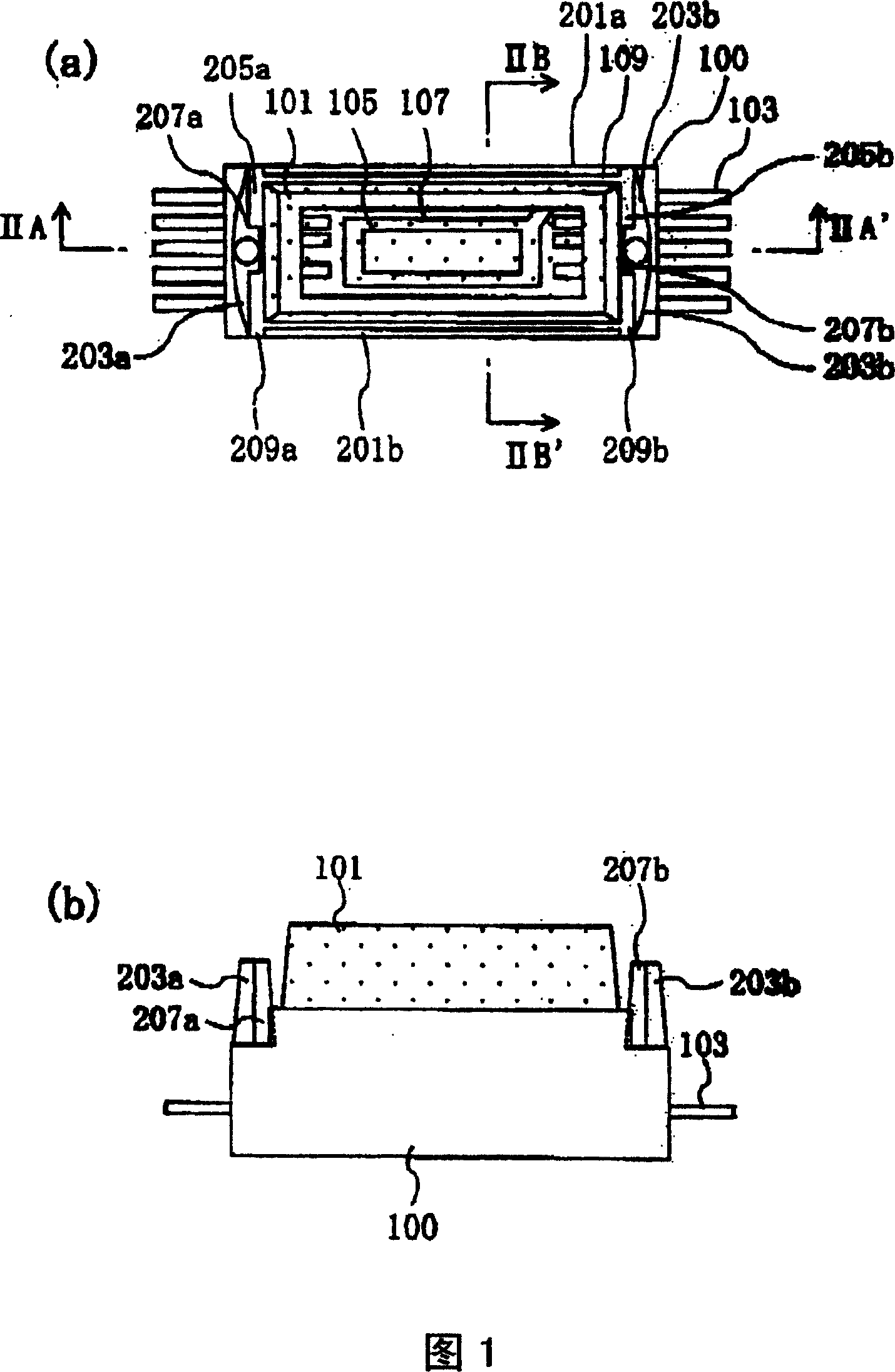
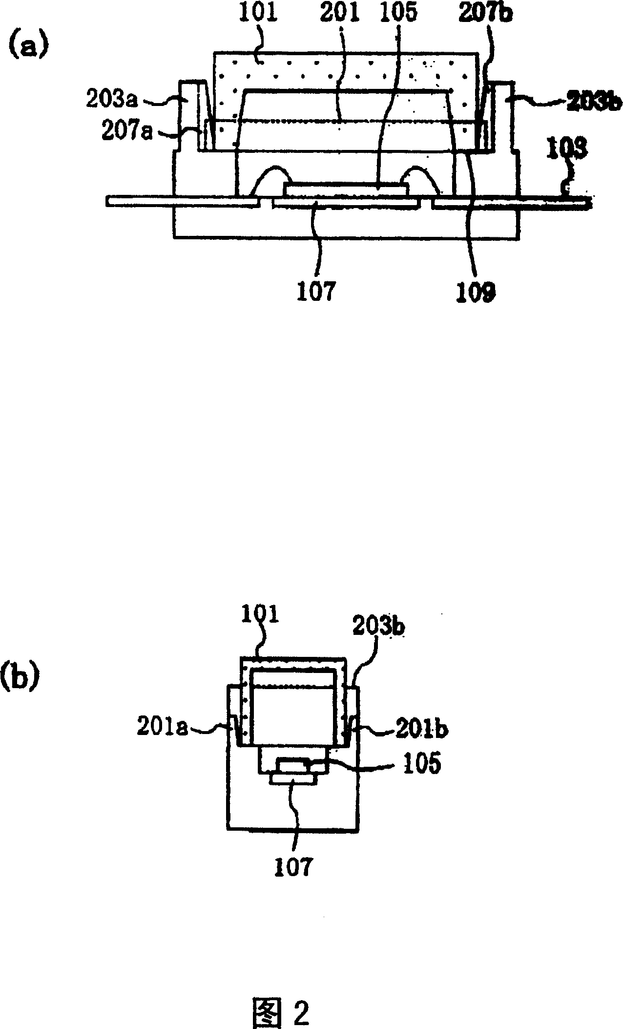
[0044] Referring to FIG. 1 and FIG. 2, an optoelectronic device according to Embodiment 1 of the present invention will be described. 1( a ) and ( b ) are a plan view and a side view showing the appearance shape of the optoelectronic device of this embodiment. 2(a) and (b) are cross-sectional structural diagrams showing lines IIA-IIA' and IIB-IIB'.
[0045] The optoelectronic device in this embodiment has an optoelectronic element 105 , a mounting portion 107 on which the optoelectronic element 105 is mounted, a resin package case 100 composed of a frame surrounding the mounting portion 107 , and an optical component 101 . The optical component 101 is placed on the optical component placement portion 109 located on the inner peripheral portion of the loading portion 107 close to the upper surface of the resin package case.
[0046] A pair of first side walls 201a, b and a pair of second side walls 203a, b are provided on the upper surface of the resin-encapsulated case. The ...
Embodiment 2
[0073] Referring to FIG. 5 and FIG. 6, an optoelectronic device according to Embodiment 2 of the present invention will be described. 5 and 6 are a plan view and a side view showing the appearance shape of the optoelectronic device of this embodiment. Fig. 6 shows the cross-sectional structure along line VI-VI' in Fig. 5 . The optoelectronic device of this example is made of the same material as that of the optoelectronic device of Example 1 above, and has almost the same shape, but differs from the structure of Example 1 in the following points. Also, the same structural parts as those of the above-mentioned embodiment 1 are omitted for simplification of description.
[0074] In the optoelectronic device of this embodiment, as shown in FIG. 5 , no sidewall cutouts [209a, b in FIG. 1(a) ] are formed between the second sidewalls 403a, b and the first sidewalls 401a, b. The reason why the sidewall notch is not formed is that the hologram element 301 is surrounded by the first ...
PUM
 Abstract
Description
Claims
Application Information
 - R&D
- Intellectual Property
- Life Sciences
- Materials
- Tech Scout
- Unparalleled Data Quality
- Higher Quality Content
- 60% Fewer Hallucinations
Browse by: Latest US Patents, China's latest patents, Technical Efficacy Thesaurus, Application Domain, Technology Topic, Popular Technical Reports.
© 2025 PatSnap. All rights reserved.Legal|Privacy policy|Modern Slavery Act Transparency Statement|Sitemap|About US| Contact US: help@patsnap.com


