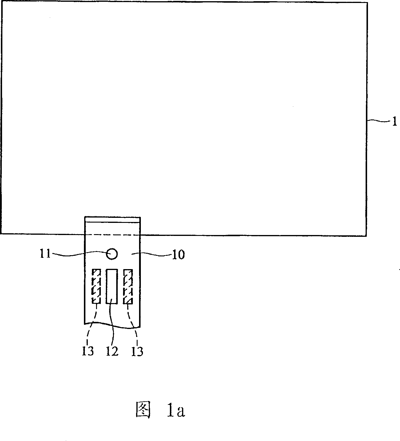
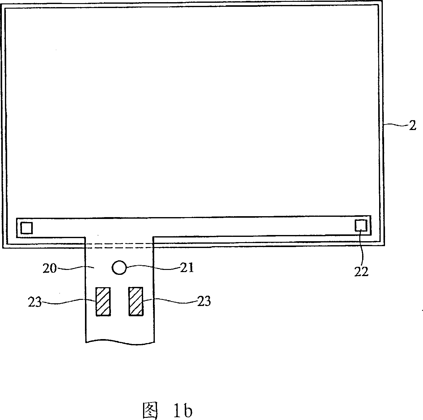
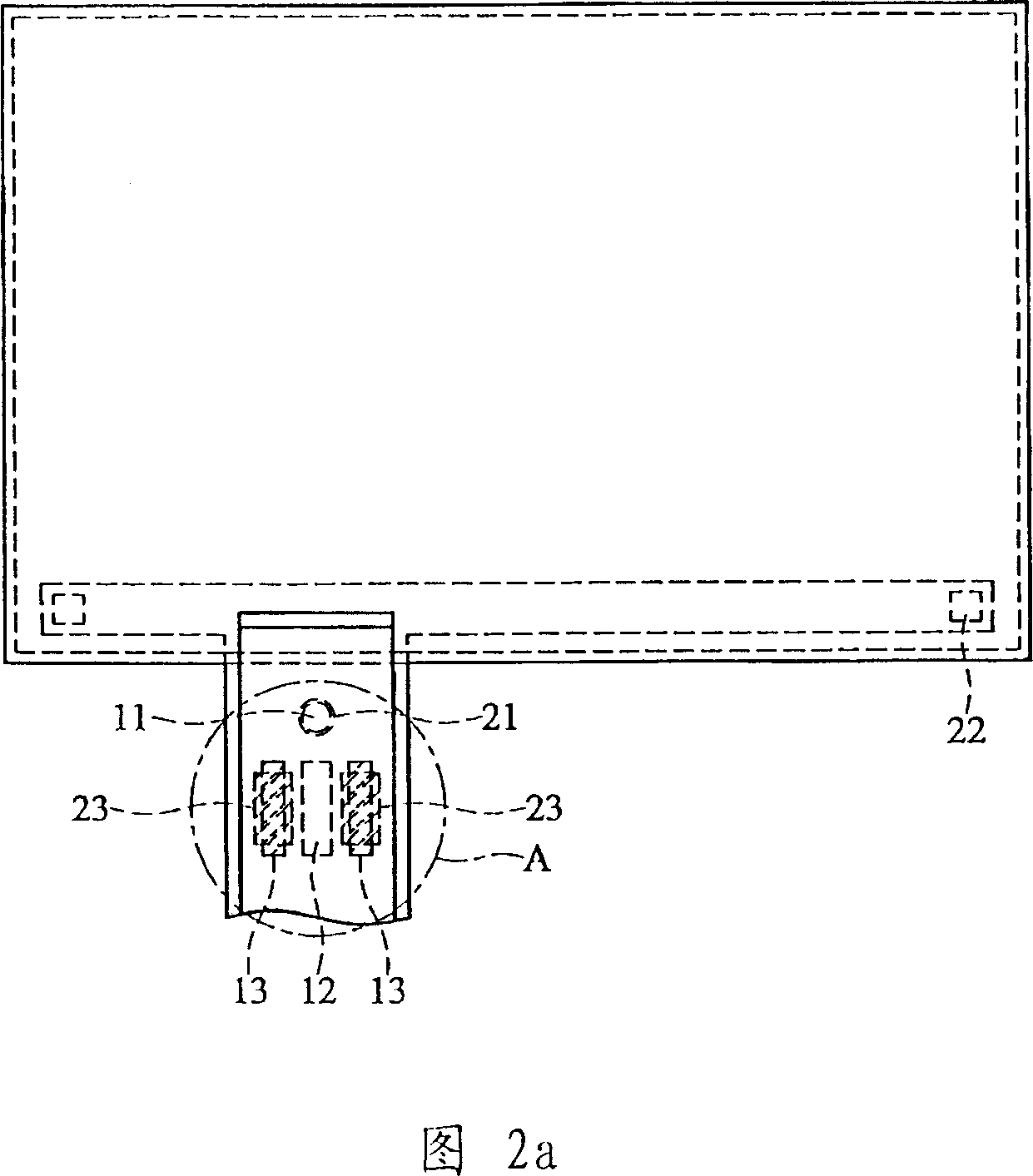
Panel display and electronic means thereof
A flat-panel display and electronic device technology, which is applied to the assembly of printed circuits, static indicators, electrical components, etc. with electrical components, can solve the problems of reduced production speed, difficult alignment of positioning holes, and time increase, etc., to achieve faster production speed Effect
- Summary
- Abstract
- Description
- Claims
- Application Information
AI Technical Summary
Problems solved by technology
Method used
Image
Examples
no. 1 example
[0053] Referring to Figure 4a, a first embodiment of the present invention is shown. FIG. 4 a shows a flexible circuit board 100 , including a base material 140 , two first soldering portions 130 , a multifunctional opening 120 and a second positioning portion 110 . The second positioning portion 110 , the multifunctional opening 120 and the first welding portion 130 are all formed on the base material 140 . The first welding portions 130 are elongated and substantially parallel to each other. The multifunctional opening 120 is strip-shaped and has an anti-overflow tin portion 121 and a first positioning portion 122 . The anti-overflow tin portion 121 is located between the first soldering portions 130 and has a length substantially equal to that of the first soldering portion 130 . The first positioning portion 122 is connected to a first side of the anti-overflow tin portion 121 . The second positioning portion 110 is located above the extension line y1 in the longitudina...
no. 2 example
[0060]Referring to Fig. 6a, it shows the second embodiment of the present invention, the difference between the second embodiment and the first embodiment is that the multifunctional opening 120 of the flexible circuit board 100 has a second positioning part 123, which is connected to the anti-overflow tin The second side of the portion 121. Referring to FIG. 6 b , the second positioning portion 123 is used to replace the second positioning portion in the first embodiment, and is opposite to the first positioning hole 211 of the circuit board.
[0061] Referring to Fig. 6c, when welding, the first positioning structure 310 is used to pass through and position the second positioning portion 123 and the first positioning hole 211 at the same time, and the second positioning structure 320 is used to pass through and position the first positioning portion 122 and the second positioning portion 123 simultaneously. positioning hole 212 . Next, the first soldering portion 130 and th...
PUM
 Abstract
Description
Claims
Application Information
 - Generate Ideas
- Intellectual Property
- Life Sciences
- Materials
- Tech Scout
- Unparalleled Data Quality
- Higher Quality Content
- 60% Fewer Hallucinations
Browse by: Latest US Patents, China's latest patents, Technical Efficacy Thesaurus, Application Domain, Technology Topic, Popular Technical Reports.
© 2025 PatSnap. All rights reserved.Legal|Privacy policy|Modern Slavery Act Transparency Statement|Sitemap|About US| Contact US: help@patsnap.com


