Dual endpoint detection for advanced phase shift and binary photomasks

a phase shift and binary technology, applied in semiconductor/solid-state device testing/measurement, instruments, electric discharge tubes, etc., can solve the problems of difficult to determine if the desired etch results are obtained for a specific photomask manufacturing process, adversely affecting performance, and completely useless masks

Active Publication Date: 2017-10-31
APPLIED MATERIALS INC
View PDF137 Cites 5 Cited by
  • Summary
  • Abstract
  • Description
  • Claims
  • Application Information

AI Technical Summary

Problems solved by technology

Thus, any defects in the mask may be transferred to the chip, potentially adversely affecting performance.
Defects that are severe enough may render the mask completely useless.
Since each photomask generally has its own set of features or patterns, different film stacks on the photomask being etched may yield different endpoint data upon different materials being used in the film stack, thereby making it difficult to determine if the desired etch results are obtained for a specific photomask manufacture process.
Accordingly, when directing a radiation to the photoresist layer and the film stack on the photomask, different thickness variation between the photoresist layer and the film stack may generate different reflective or transmissive signal to the endpoint data, therefore, making it even more difficult to determine an accurate endpoint for both the photoresist layer and the photomask etching process without interfered by the photoresist thickness variation.

Method used


Image

  • Dual endpoint detection for advanced phase shift and binary photomasks
  • Dual endpoint detection for advanced phase shift and binary photomasks
  • Dual endpoint detection for advanced phase shift and binary photomasks

Examples


Embodiment Construction

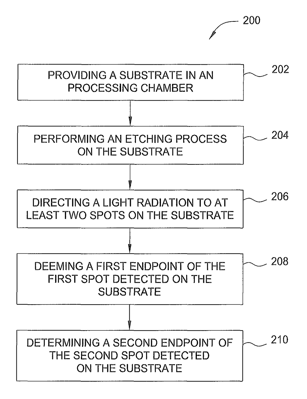
[0022]The present invention provides a method and apparatus for etching a photomask substrate with enhanced process monitoring, for example, by providing for optical monitoring at certain regions of the photomask to obtain desired etch rate or endpoint determination for both a photoresist layer and an absorber layer disposed on the photomask substrate. Although the discussions and illustrative examples focus on the etching rate detection, thickness loss and process endpoint determination during an etching process of a photoresist layer and an absorber layer disposed on a photomask substrate, various embodiments of the invention can also be adapted for process monitoring of other suitable substrates, including transparent substrates, or dielectric substrates and optical disks. Although the discussions and illustrative examples focus on the etching of a photomask structure, various embodiments of the invention can also be adapted for process monitoring of other suitable substrates, in...


PUM

PropertyMeasurementUnit
wavelengthaaaaaaaaaa

Abstract

The present invention provides a method and apparatus for etching a photomask substrate with enhanced process monitoring, for example, by providing for optical monitoring at certain regions of the photomask to obtain dual endpoints, e.g., etch rate or thickness loss of both a photoresist layer and an absorber layer. By monitoring transmissity of an optical beam transmitted through areas having photoresist layer and etched absorber layer at two different predetermined wavelength, dual process endpoints may be obtained by a signal optical detection.

Description

RELATED APPLICATIONS[0001]This application claims priority to U.S. Provisional Patent Application Ser. No. 61 / 713,185 filed on Oct. 12, 2012, and U.S. Provisional Patent Application Ser. No. 61 / 749,156, filed on Jan. 4, 2013, both of which are incorporated by reference in their entireties.BACKGROUND OF THE INVENTION[0002]Field of the Invention[0003]Embodiments of the present invention generally relate to methods to detect endpoints for both a photoresist layer and an absorber layer in an etching process for the fabrication of photomasks useful in the manufacture of integrated circuits.[0004]Description of the Related Art[0005]In the manufacture of integrated circuits (IC), or chips, patterns representing different layers of the chip are created by a chip designer. A series of reusable masks, or photomasks, are created from these patterns in order to transfer the design of each chip layer onto a semiconductor substrate during the manufacturing process. Mask pattern generation systems...

Claims


Application Information

Patent Timeline
Patent Type & Authority Patents(United States)
IPC IPC(8): H01L21/306H01J37/32G03F1/26H01L21/3065G03F1/80H01L21/66H01L21/308
CPCH01L21/3065G03F1/26G03F1/80H01L22/20H01L21/3085H01L22/12H01J37/32963
Inventor GRIMBERGEN, MICHAEL N.
Owner APPLIED MATERIALS INC
Why Eureka
Try Eureka