
Wafer carrier

a technology of wafers and carriers, applied in the field of wafer carriers, can solve the problems of no suitable substrate available for use, no suitable substrate available, and warp in the epitaxial layer

Active Publication Date: 2017-06-27
EPISTAR CORP
View PDF60 Cites 217 Cited by
  • Summary
  • Abstract
  • Description
  • Claims
  • Application Information

AI Technical Summary

Benefits of technology

The present patent describes a wafer carrier and a manufacturing method. The wafer carrier has a supporting body with an opening and a curved bottom surface, and a plurality of supporting rods formed around the periphery of the supporting body. The method involves measuring the curvature radius of the wafer structure and providing the wafer carrier accordingly. The technical effect of the invention is to provide a wafer carrier that can securely hold and protect wafers during transportation without causing damage, yield loss, or contamination.

Problems solved by technology

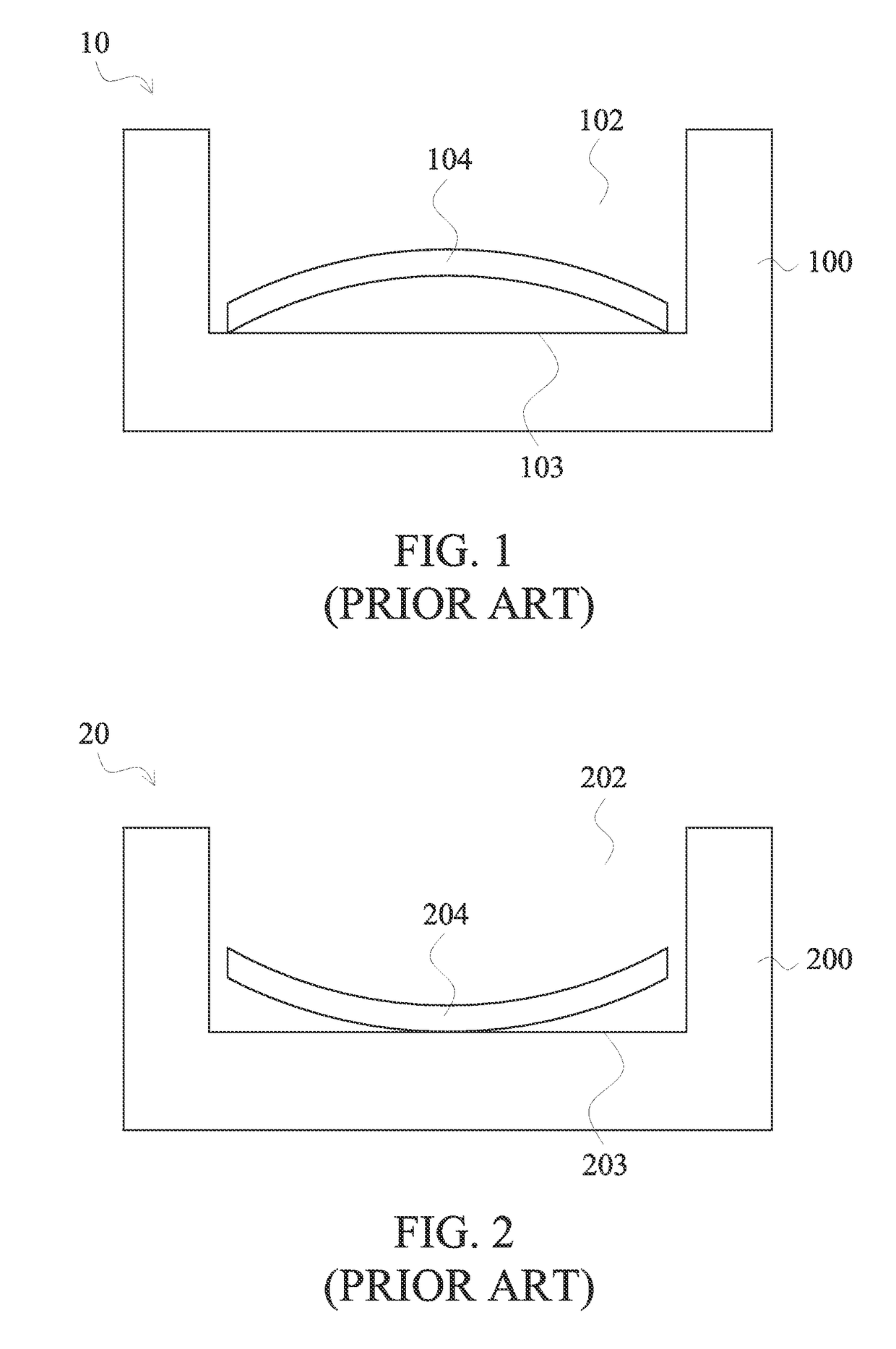
The stress affects the epitaxial quality of the epitaxial layer, and the stress may result in warp in the epitaxial layer.
However, for some epitaxial layers, there is no suitable substrate available for use, neither the same material as the epitaxial layer, nor the same lattice constant as the epitaxial layer.
Further, in consideration of the cost of the production, there may be no suitable substrate available.
Mild stress may result in uneven heating of the epitaxial layer, which further results in poor epitaxial quality.
However, if the stress is too large, the epitaxial layer may rupture.
When the wafer structure is bowed, the wafer cannot contact with the wafer carrier closely, which results in uneven temperature distribution across the whole wafer surface.

Method used


Image

  • Wafer carrier
  • Wafer carrier
  • Wafer carrier

Examples


first embodiment

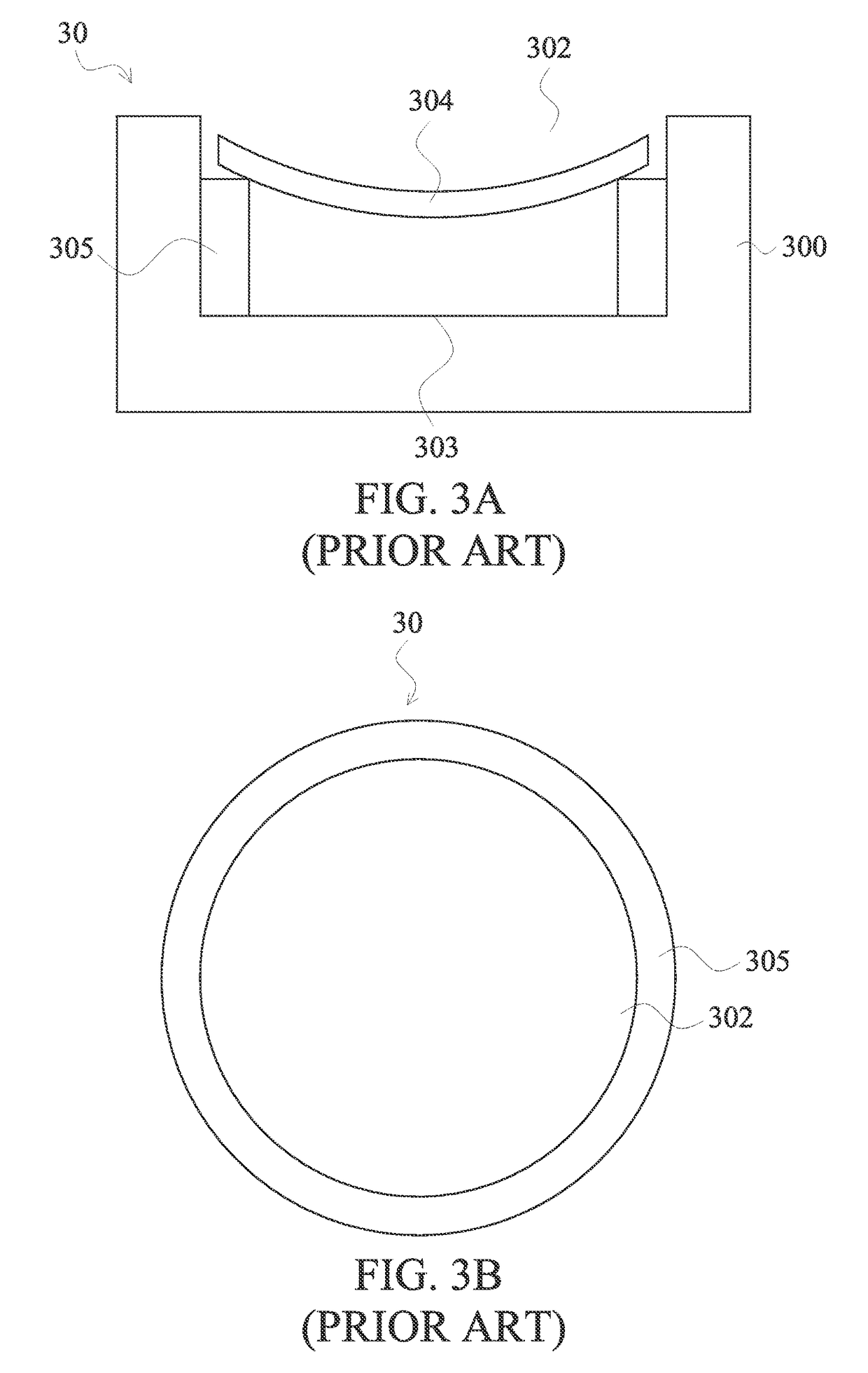
[0027]FIG. 4A illustrates a cross-sectional view of a wafer carrier 40 in accordance with the present application. As shown in FIG. 4A, the wafer carrier 40 comprises a supporting body 400 having a height 401; and a plurality of supporting rods 405 formed around a periphery of the supporting body 400. The supporting body 400 comprises an opening 402, wherein a bottom surface 403 of the opening 402 is a curved surface.

[0028]A top view of the opening 402 of the wafer carrier 40 is approximately a circle shape. The opening 402 can accommodate a commercial wafer having a diameter between 2 in and 8 in. The top view of the wafer carrier 40 can be referred to FIG. 8A. FIG. 8A illustrates a top view of a wafer carrier 80 in accordance with an embodiment of the present application. If the wafer carrier 80 is used to support a wafer having a diameter of 4 in or above, the top view of the opening (not shown) of the wafer carrier 80 further comprises a flat edge 803. As shown in FIG. 4A, a waf...

second embodiment

[0036]FIG. 5A illustrates a cross-sectional view of a wafer carrier 50 in accordance with the present application. As shown in FIG. 5A, the wafer carrier 50 comprises a supporting body 500 having a height 501; and a plurality of supporting rods 505 formed around a periphery of the supporting body 500. The supporting body 500 comprises an opening 502, wherein a bottom surface 503 of the opening 502 is a curved surface.

[0037]A top view of the opening 502 of the wafer carrier 50 is approximately a circle shape. The opening 502 can accommodate a commercial wafer having a diameter between 2 in and 8 in. The top view of the wafer carrier 50 can be referred to FIG. 8A. FIG. 8A illustrates a top view of a wafer carrier 80 in accordance with an embodiment of the present application. If the wafer carrier 80 is used to support a wafer having a diameter of 4 in or above, the top view of the opening (not shown) of the wafer carrier 80 further comprises a flat edge803. As shown in FIG. 5A, a wafe...


PUM

PropertyMeasurementUnit
heightsaaaaaaaaaa
heightsaaaaaaaaaa
diameteraaaaaaaaaa

Abstract

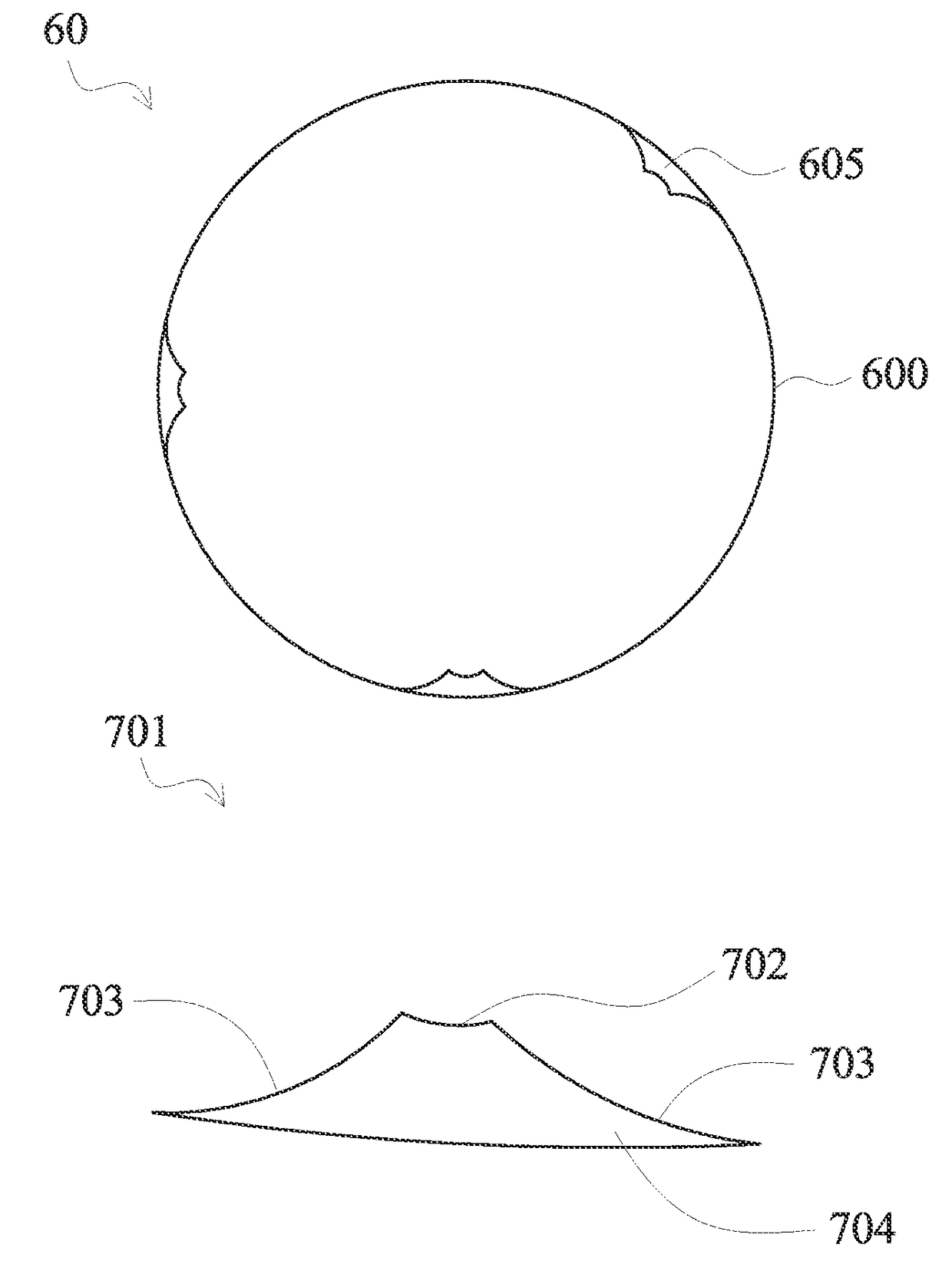
A wafer carrier comprises a supporting body having an opening therein, wherein said opening in said supporting body has a concave sidewall and a bottom surface in said supporting body which is curved in cross section; a plurality of vertical supporting rods configured to support and contact a wafer received in said opening and to displace said wafer from the bottom surface of the opening in said supporting body; wherein one of said supporting rods has an end for contacting and supporting said wafer; and wherein when viewing from a top view of the wafer carrier, one of said supporting rods has a base lining on the concave sidewall of said opening in said supporting body, a first concave side opposite to the base and two second concave sides connecting the base and the first concave side.

Description

TECHNICAL FIELD[0001]The application relates to a wafer carrier, and more particularly, to a wafer carrier having a supporting body and a plurality of supporting rods formed around a periphery of the supporting body.REFERENCE TO RELATED APPLICATION[0002]This application claims the right of priority based on Taiwan application Serial No. 100137510, filed on Oct. 14, 2011, and the content of which is hereby incorporated by reference in its entirety.DESCRIPTION OF BACKGROUND ART[0003]In the manufacturing of a light-emitting diode (LED), an epitaxial layer is grown on a substrate. The substrate functions as a seed layer. When the lattice constant of the substrate is similar to the lattice constant of the epitaxial layer, a defect such as dislocation between the epitaxial layer and the substrate can be reduced. When the epitaxial layer is formed on the substrate, a stress is formed between the epitaxial layer and the substrate under different temperature regions of the reactor furnace. T...

Claims


Application Information

Patent Timeline
Patent Type & Authority Patents(United States)
IPC IPC(8): H01L21/67H01L21/687C23C16/458H01L21/66H01L21/683
CPCH01L22/12C23C16/4585H01L21/683H01L21/67
Inventor CHANG, CHUNG-YINGLO, YUN-MINGSHEN, CHITSENG, YING-CHAN
Owner EPISTAR CORP
Learn More