
Array substrate and organic light-emitting display including the same

a technology of organic light-emitting display and substrate, which is applied in the direction of organic semiconductor devices, semiconductor/solid-state device details, radiation controlled devices, etc., can solve the problems of reducing the reliability of the display area and creating cracks in the substra

Active Publication Date: 2016-10-18
SAMSUNG DISPLAY CO LTD
View PDF16 Cites 18 Cited by
  • Summary
  • Abstract
  • Description
  • Claims
  • Application Information

AI Technical Summary

Benefits of technology

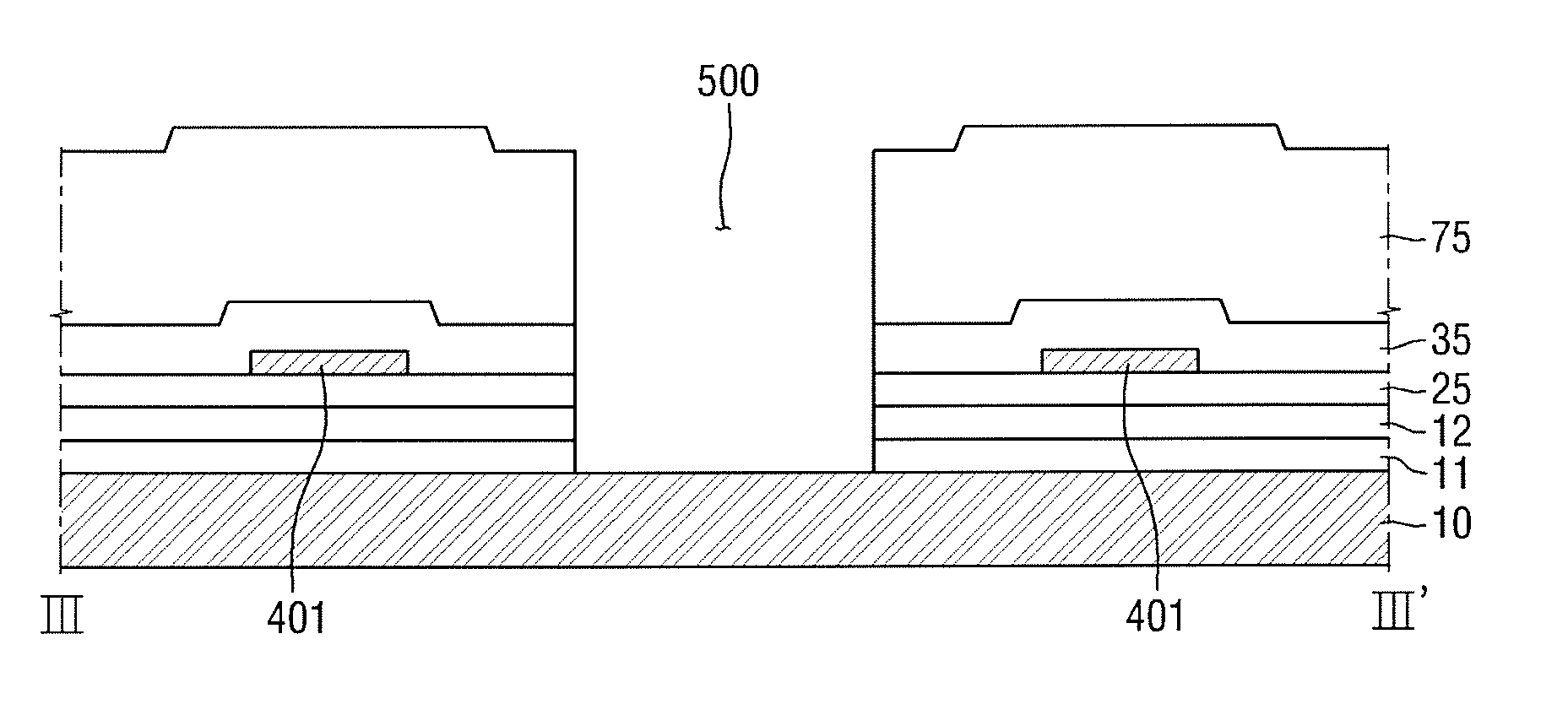
[0009]Exemplary embodiments of the present invention provide an array substrate structured to prevent the creation of cracks.
[0010]Exemplary embodiments of the present invention also provide an array substrate structured to suppress the propagation of cracks.
[0011]Exemplary embodiments of the present invention also provide an organic light-emitting display (OLED) structured to prevent the creation of cracks.
[0012]Exemplary embodiments of the present invention also provided an OLED structured to suppress the propagation of cracks.

Problems solved by technology

These impacts may create cracks in the substrate.
That is, when cracks are created in a part of the non-display area, they may propagate to the display area along the inorganic insulating layers, thereby degrading the reliability of the display area.

Method used


Image

  • Array substrate and organic light-emitting display including the same
  • Array substrate and organic light-emitting display including the same
  • Array substrate and organic light-emitting display including the same

Examples


Embodiment Construction

[0052]Exemplary embodiments of the present invention and methods for achieving the aspects and features will be apparent by referring to the embodiments to be described in detail with reference to the accompanying drawings. However, exemplary embodiments of the present invention are not limited to the embodiments disclosed hereinafter, but can be implemented in diverse forms.

[0053]In the entire description of the present invention, the same drawing reference numerals are used for the same elements across various figures.

[0054]In the drawings, the thickness of layers, films, panels, regions, etc., may be exaggerated for clarity. It will be understood that when an element such as a layer, film, region, or substrate is referred to as being “on” another element, it can be directly on the other element or intervening elements may also be present.

[0055]As used herein, the singular forms, “a”, “an”, and “the” are intended to include plural forms as well, unless the context clearly indicate...


PUM


Abstract

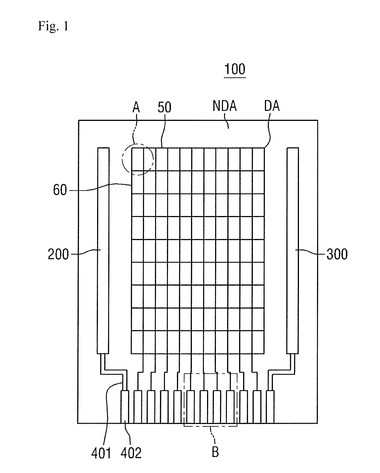
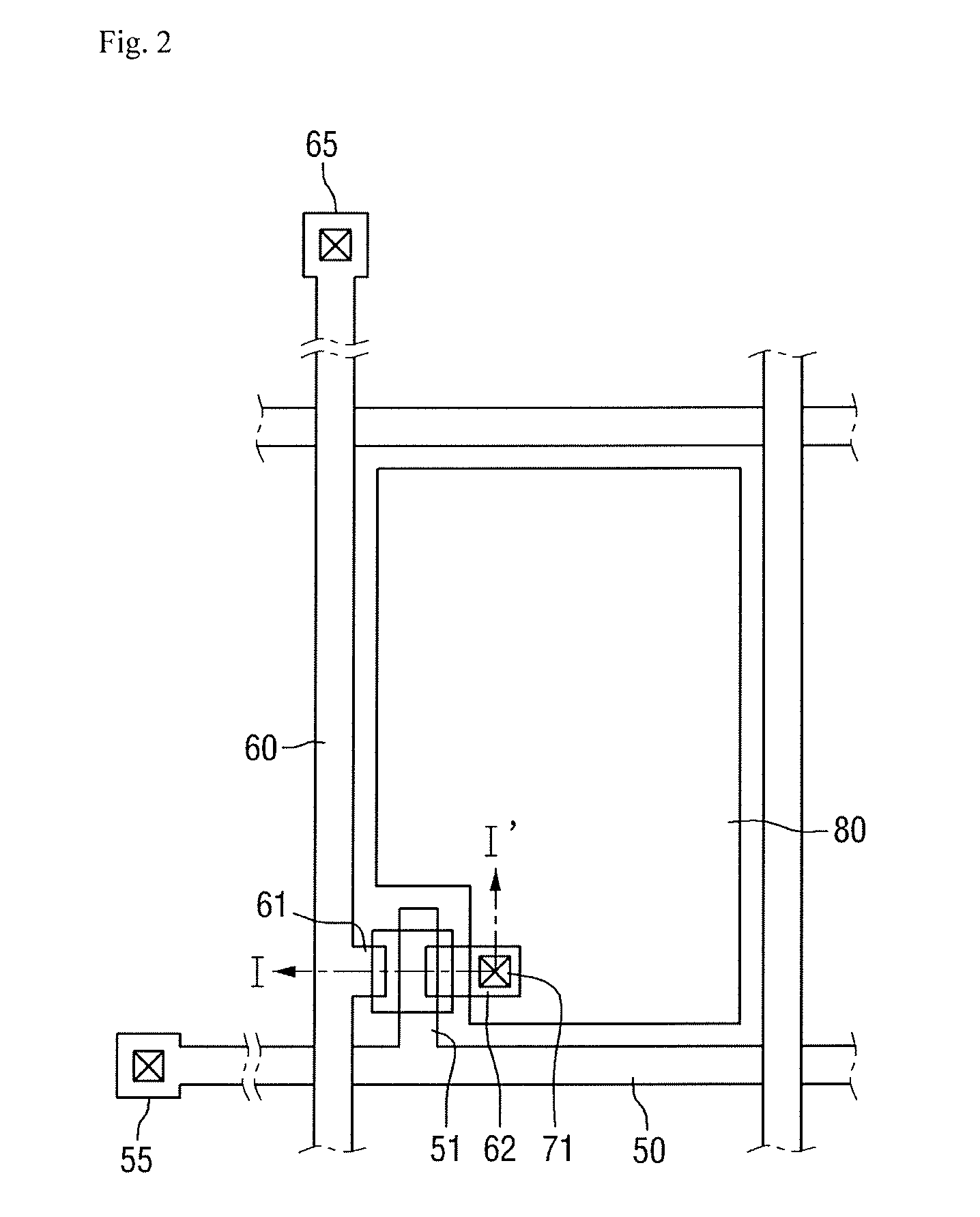
An array substrate includes a substrate, a barrier layer disposed on the substrate, a buffer layer disposed on the barrier layer, a first insulating layer disposed on the buffer layer, a second insulating layer disposed on the first insulating layer, a plurality of wiring patterns disposed between the first insulating layer and the second insulating layer and / or on the second insulating layer. In addition, the wiring patterns are separated from each other, and extend toward a side of the substrate. The array substrate further includes a recess pattern disposed adjacent the wiring patterns and recessed from a top surface of the second insulating layer to expose at least part of a top surface of the substrate, and an organic insulating layer disposed on the second insulating layer and exposing at least part of a portion of the top surface of the substrate which is exposed by the recess pattern.

Description

[0001]This application claims priority to Korean Patent Application No. 10-2013-0069039 filed on Jun. 17, 2013 and Korean Patent Application No. 10-2013-0125416 filed on Oct. 21, 2013, the disclosures of which are hereby incorporated by reference herein in their entireties.BACKGROUND OF THE INVENTION[0002]1. Technical Field[0003]The present disclosure relates to an array substrate and a display device including the same, and more particularly, to an array substrate having a display area and a non-display area and a display device including the array substrate.[0004]2. Discussion of the Related Art[0005]A display device such as a liquid crystal display (LCD) or an organic light-emitting display (OLED) may include an array substrate having a display area and a non-display area located outside the display area. Such a display device may include a plurality of pixels in the display area as basic elements for displaying an image, and each of the pixels may include a switching device to o...

Claims


Application Information

Patent Timeline
Patent Type & Authority Patents(United States)
IPC IPC(8): H01L27/146H01L23/00H01L27/32H01L27/12
CPCH01L23/562H01L27/124H01L27/1218H01L27/1244H01L27/3276H01L2251/5338H01L2924/0002H01L2924/00H01L23/13H01L23/145H10K50/8426H10K59/131H10K2102/311
Inventor KWAK, WON KYU
Owner SAMSUNG DISPLAY CO LTD
Learn More