Display device

a display device and display technology, applied in the field of display devices, can solve the problems of low aperture ratio, voltage drop, and potential of power supply not always kept constant, and achieve the effect of simplifying configuration without increasing power consumption and wiring in the pixel circuit, and avoiding voltage drop

Active Publication Date: 2016-06-07
SHARP KK
View PDF17 Cites 5 Cited by
  • Summary
  • Abstract
  • Description
  • Claims
  • Application Information

AI Technical Summary

Benefits of technology

[0044]In the first aspect of the present invention, the tone voltage generation portion calculates a voltage drop amount of the power line due to an image being displayed, on the basis of tone values indicating display luminances of a plurality of pixels, and sets reference voltages on the basis of the calculated voltage drop amount, so that it is possible to eliminate the need to apply a detection current in order to detect a voltage drop amount, resulting in no increase in power consumption, it is also possible to eliminate the need to provide wiring for voltage drop amount detection, resulting in no increase in the wiring in the pixel circuits is not increased, and it is possible to compensate for voltage drops with accuracy.
[0045]In the second aspect of the present invention, tone values are integrated, and a voltage drop amount is calculated on the basis of the resultant value, so that it is possible to compensate for voltage drops with accuracy using a simplified configuration without increasing power consumption and the wiring in the pixel circuits.
[0046]In the third aspect of the present invention, the maximum and minimum values for tone voltages are set as reference voltages, and the tone voltages are generated and outputted on the basis of the maximum and minimum value, so that it is possible to compensate for voltage drops using a simplified configuration without requiring a specialized circuit configuration.
[0047]In the fourth aspect of the present invention, at least one of the maximum and minimum values is set for each primary color, a tone voltage value is generated and outputted for each primary color, and therefore, in the case where she pixel circuit configuration varies among the colors, typically, in the case where the configuration of the means for driving an electro-optical element varies among them, it is possible to provide an appropriate tone voltage for each color in accordance with the configuration of the pixel circuit for that color, thereby compensating for the voltage drop with higher accuracy and improving display quality.
[0048]In the fifth aspect of the present invention, the tone values are integrated for each primary color, the voltage drop amount is calculated for each primary color on the basis of the resultant value for that color, and therefore, it is possible to compensate for the voltage drop for each color with higher accuracy.
[0049]In the sixth aspect of the present invention, the power line is provided for each primary color, corresponding power supply voltages are provided to the power lines provided for the respective primary colors, and therefore, voltage drops occur without any interference between the power lines. Therefore, it is possible to reduce the voltage drop amount itself for each power line, and compensate for the voltage drop for each color with higher accuracy.

Problems solved by technology

However, the constant-current control mode is known to require more drive transistors and more wiring lines than the constant-voltage control mode, which leads to a lower aperture ratio, and therefore, the constant-voltage control mode is widely employed.
In such a configuration employing the constant-voltage control mode, the current to be applied to the organic EL element is determined by the drive (control) transistor, but the potential of the power supply is not always kept constant, and might experience a voltage drop (i.e., an IR drop) due to the resistance of a power supply line and the current flowing through the line.
Particularly in the case of an image where the average tone value of the pixels to be displayed is high (a bright image), the current flowing through the power supply line increases, and therefore, the control voltage of the drive transistor is affected by the aforementioned voltage drop, resulting in a further drop in the voltage, leading to a reduction in display quality, such as deviations in the colors of the image to be displayed or portions with low tones being darkened.

Method used


Image

  • Display device
  • Display device
  • Display device

Examples


first embodiment

1. First Embodiment

1.1 Overall Configuration

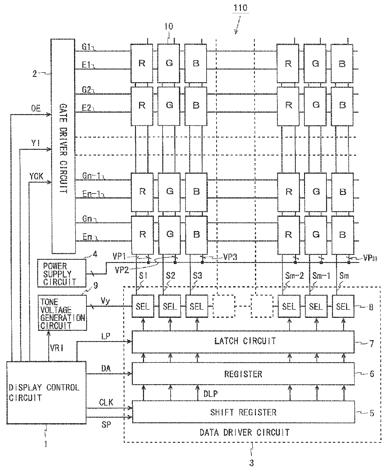
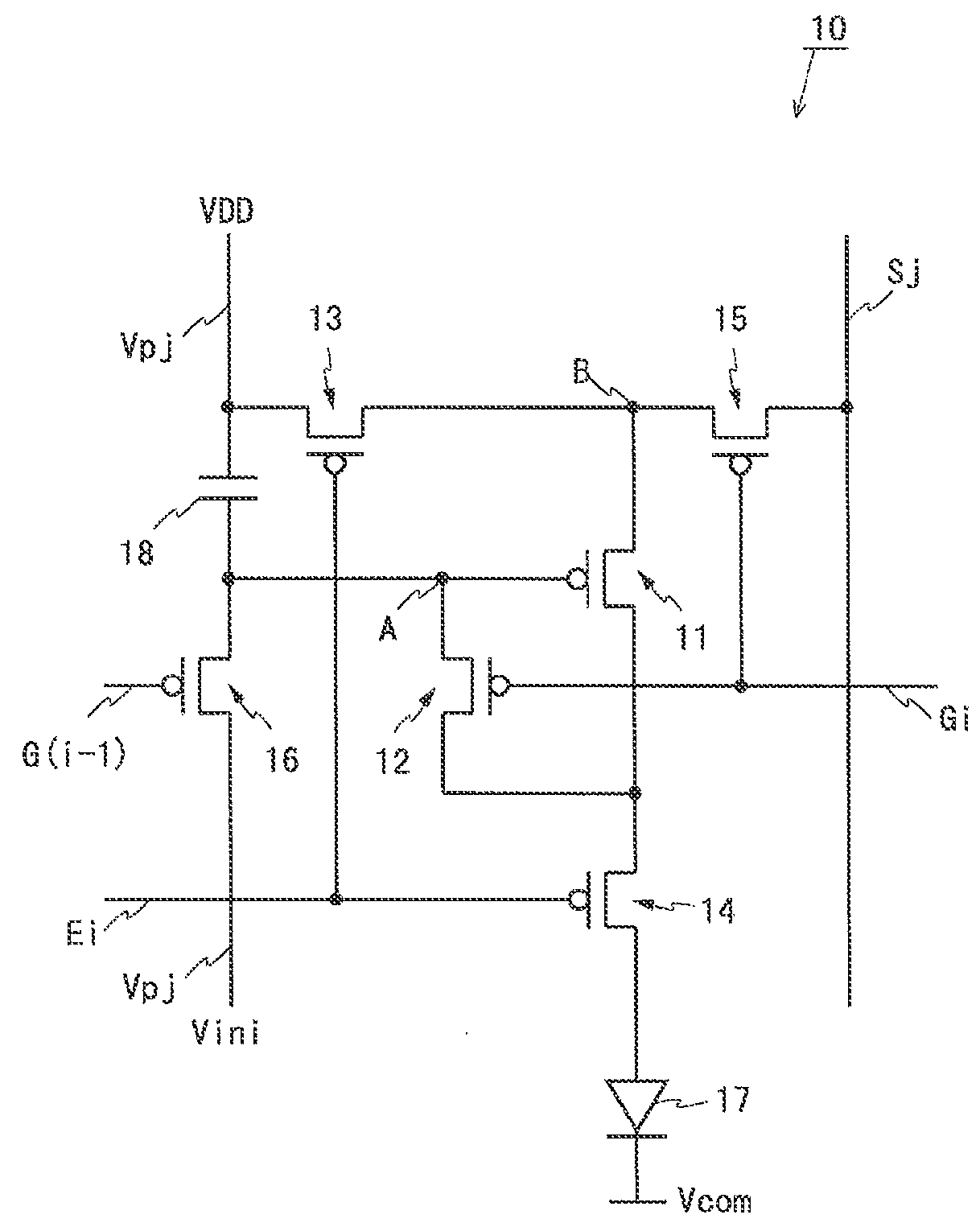
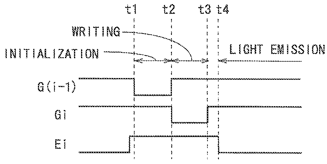
[0078]FIG. 1 is a block diagram illustrating the configuration of a display device according to a first embodiment of the present invention. The display device 110 shown in FIG. 1 is an organic EL display including a display control circuit 1, a gate driver circuit 2, a data driver circuit 3, a power supply circuit 4, a tone voltage generation circuit 9, and (m×n) pixel circuits 10. In the following, m and n are integers of 2 or more, i is an integer greater than or equal to 1 but less than or equal to n, and j is an integer greater than or equal to 1 but less than or equal to m.

[0079]The display device 110 is provided with a parallel scanning signal lines Gi and m parallel data lines Sj perpendicular thereto. Although omitted in the figure, there are further provided scanning signal lines G0 for initialization control to be described later. The (m×n) pixel circuits 10 are arranged in a matrix corresponding to the intersections of the scan...

second embodiment

2. Second Embodiment

2.1 Overall Configuration

[0141]FIG. 12 is a block diagram illustrating the configuration of a display device according to a second embodiment of the present invention. The display device 120 shown in FIG. 12 has approximately the same configuration as the display device 110 of the first embodiment shown in FIG. 1, therefore the same components will be denoted by the same characters, and any descriptions thereof will be omitted. In the present embodiment, a tone voltage generation circuit 95 has a different configuration from that of the tone voltage generation circuit 9 in the first embodiment. Therefore, the configuration and the operation of the tone voltage generation circuit 95 will be described below with reference to FIGS. 13 and 14.

2.2 Configuration of the Tone Voltage Generation Circuit

[0142]FIG. 13 is a block diagram illustrating in detail the configuration of the tone voltage generation circuit. The tone voltage generation circuit 95 shown in FIG. 13 in...

third embodiment

3. Third Embodiment

3.1 Overall. Configuration

[0153]FIG. 20 is a block diagram illustrating the configuration of a display device according to a third embodiment of the present invention. The display device 130 shown in FIG. 20 has approximately the same configuration as the display device 120 in the second embodiment shown in FIG. 12, therefore the same components will be denoted by the same reference characters, and any descriptions thereof will be omitted. In the present embodiment, when compared to the second embodiment, the voltage drop amount calculation portion 30 and the tone voltage generation circuit 95 have slightly different configurations, and the power supply circuit 45 and the power wiring have significantly different configurations.

[0154]More specifically, the power supply circuit 45 includes an R pixel power line VPr coupled only to R pixels, a G pixel power line VPg coupled only to G pixels, and a B pixel power line VPb coupled only to B pixels, and these power line...


PUM


Abstract

In a display device (110) provided with pixel circuits including organic EL elements, a display control circuit (1) calculates a voltage drop amount VRI of a power line due to display for each frame on the basis of an integrated value for display data, and a tone voltage generation circuit (9) adjusts reference voltages for a tone voltage on the basis of the integrated value in order to compensate for the voltage drop amount VRI. As a result, it is possible to compensate for the voltage drop of the power line with accuracy without increasing power consumption and the wiring in the pixel circuits.

Description

CROSS REFERENCE TO RELATED APPLICATIONS[0001]This is a U.S. National Phase patent application of PCT / JP2013 / 055310, filed Feb. 28, 2013, which claims priority to Japanese patent application no. 2012-057271 filed Mar. 14, 2012, each of which is hereby incorporated by reference in the present disclosure in its entirety.TECHNICAL FIELD[0002]The present invention relates to display devices, and more specifically, the invention relates to a display device, such as an organic EL display, which includes light-emitting display elements driven by a current, and a method for driving the same.BACKGROUND ART[0003]Organic EL (electroluminescent) displays are conventionally known as being thin display devices featuring high image quality and low power consumption. The organic EL display has a plurality of pixel circuits arranged in a matrix, each circuit including an organic EL element, which is a light-emitting display element driven by a current, and a drive transistor for driving the element.[...

Claims


Application Information

Patent Timeline
Patent Type & Authority Patents(United States)
IPC IPC(8): G09G5/10G09G3/20G09G3/32G09G5/02H01L51/50
CPCG09G3/2003G09G3/3208G09G3/3258G09G5/02G09G2300/0819G09G2300/0861G09G2320/0223G09G2320/0242G09G2320/0271G09G2320/0666G09G2320/0673G09G2330/023H01L51/50H10K50/00
Inventor TAKAHAMA, KENGOYAMANAKA, SHIGETSUGU
Owner SHARP KK
Why Eureka
Try Eureka