Apparatus and method for temperature compensated gain and mismatch trim in subranging quantizers and analog to digital converters

a temperature-compensated gain and mismatch trim technology, applied in the field of electronic circuits, can solve the problems of reducing the resolution of flash adcs, reducing the performance of flash adcs, and adding significant cost to the final produ

Active Publication Date: 2015-12-15
LOCKHEED MARTIN CORP
View PDF4 Cites 14 Cited by
  • Summary
  • Abstract
  • Description
  • Claims
  • Application Information

AI Technical Summary

Benefits of technology

The patent describes a method for compensating for temperature changes in an analog to digital converter (ADC) by using a temperature compensated reference current. This reference current is produced by a current source and then copied to a current mirror, which in turn outputs a fractional portion of the reference current to a trim digital to analog converter (DAC). The output of the DAC is then combined with the original reference current to produce an adjusted reference current. This adjusted reference current is then applied to a replica resistor ladder to produce desired voltage levels. The method also includes using a plurality of pipelined quantizing stages and a mismatch trim current circuit to compensate for errors in the DAC components. The technical effect of this patent is to improve the accuracy and reliability of analog to digital conversion in various applications such as temperature compensation in industrial control systems.

Problems solved by technology

Flash ADCs are generally limited to 8 bits of resolution.
However, these trimming methods introduce a non-temperature compensated offset to the voltages which degrades performance.
Laser trimming requires additional manufacturing steps and more robust measurement techniques during production and therefore adds significant cost to the final product.

Method used


Image

  • Apparatus and method for temperature compensated gain and mismatch trim in subranging quantizers and analog to digital converters
  • Apparatus and method for temperature compensated gain and mismatch trim in subranging quantizers and analog to digital converters
  • Apparatus and method for temperature compensated gain and mismatch trim in subranging quantizers and analog to digital converters

Examples


Embodiment Construction

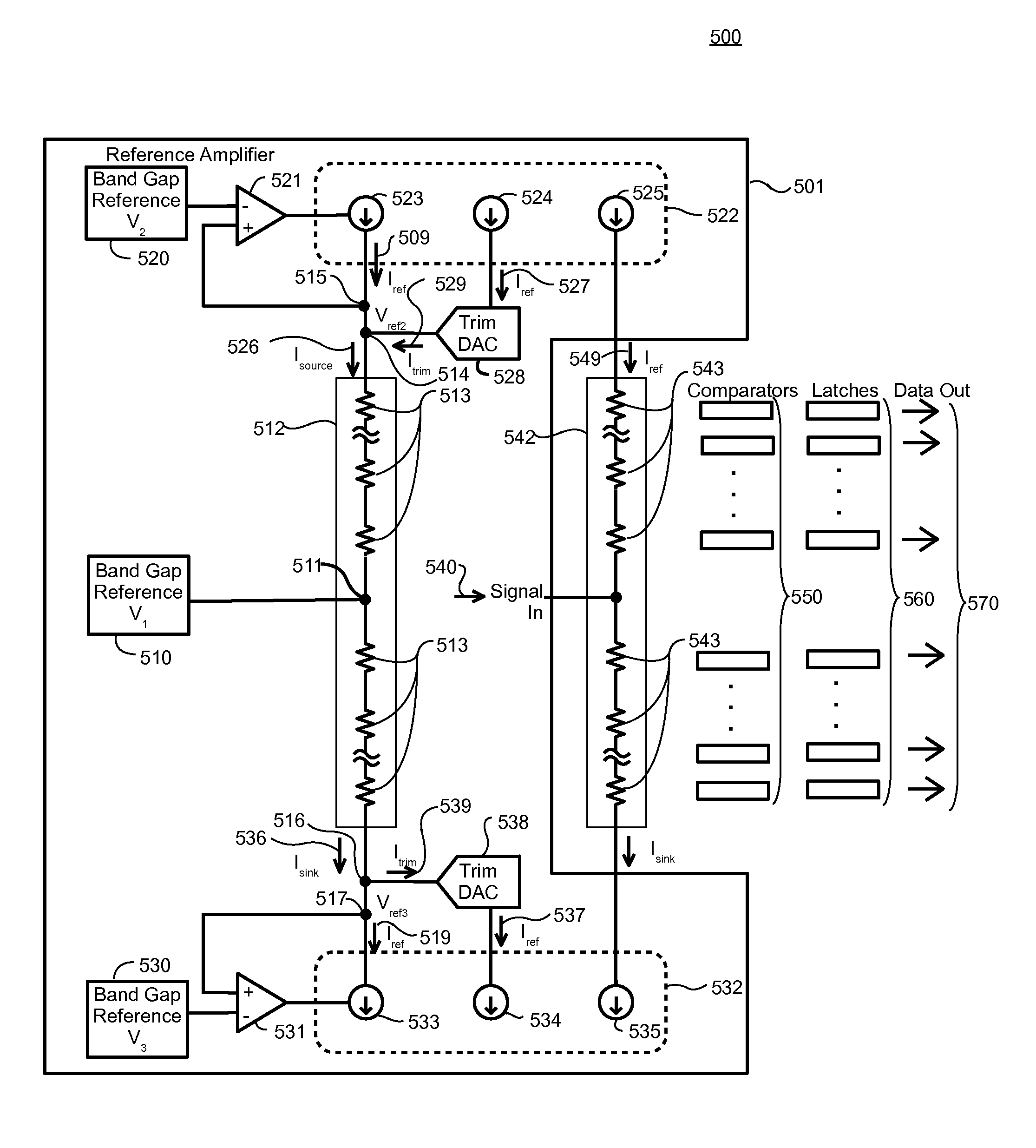
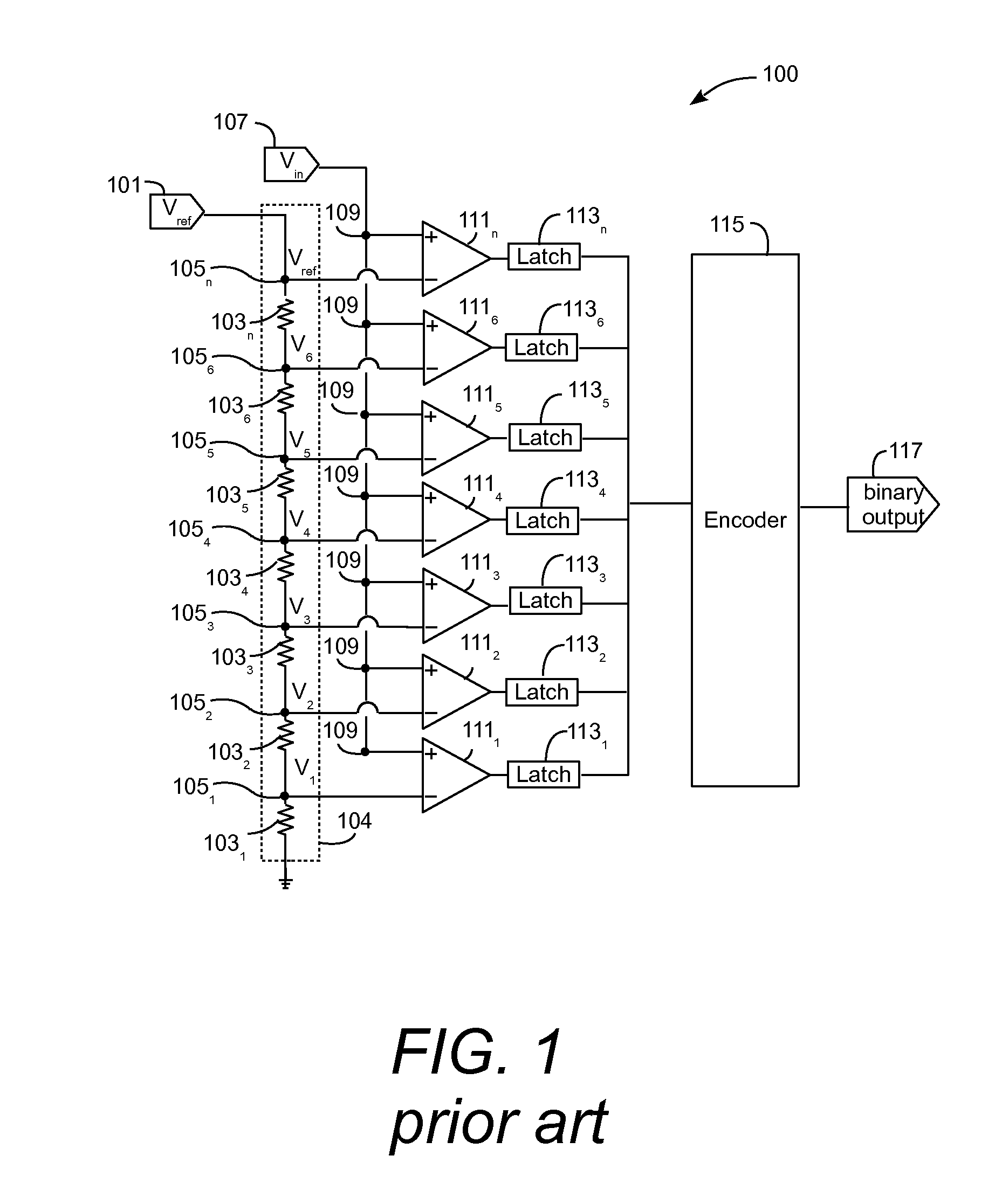
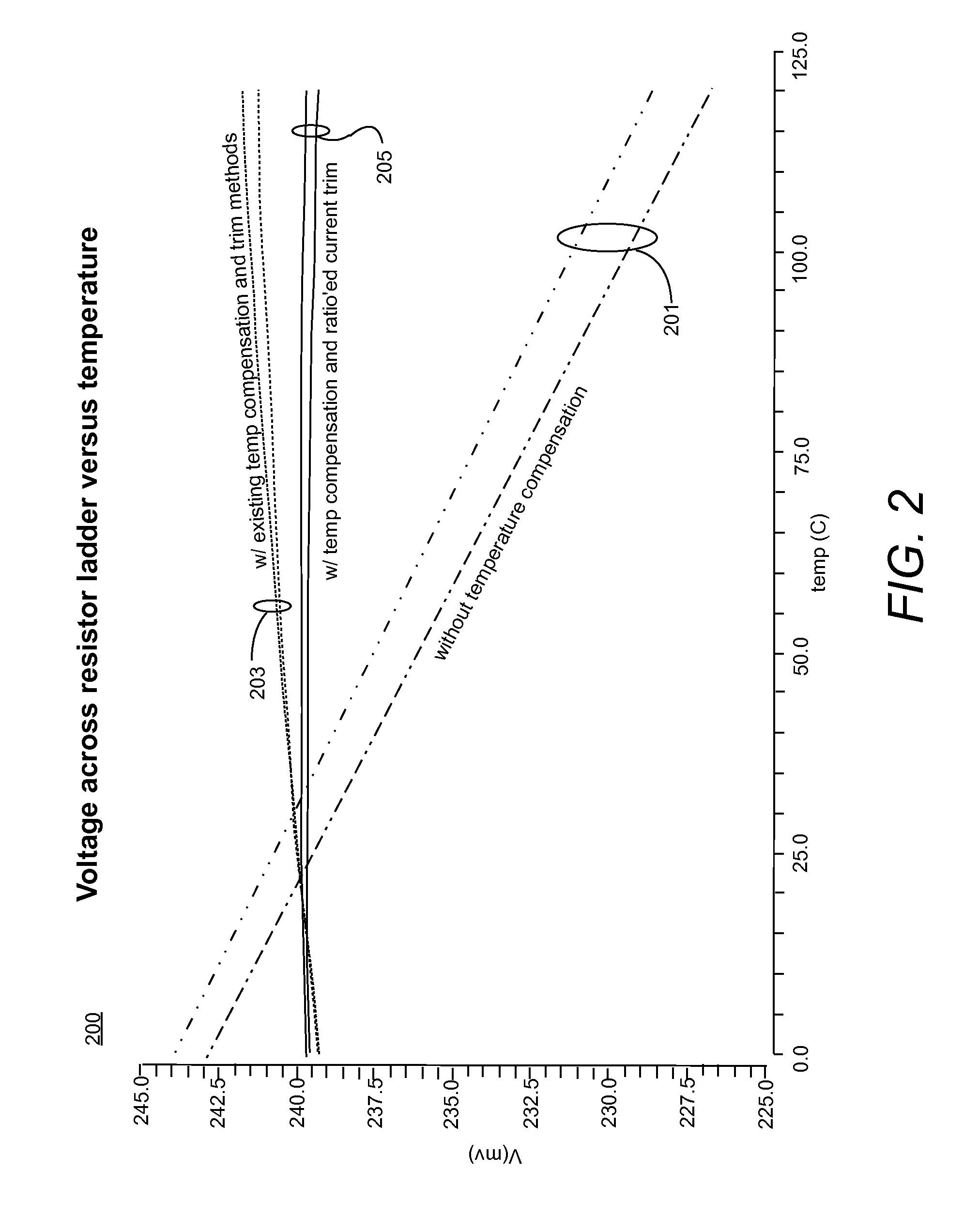
[0019]A flash analog to digital converter (ADC) requires a temperature compensated reference current in order to generate stable voltage drops across the architecture's quantizing resistor ladder. This is generally accomplished through replica biasing using a replica resistor ladder. In addition, voltage drops in the actual or output resistor ladder must be trimmed to the appropriate voltages to account for process variations. Conventional methods introduce a non-temperature compensated offset to the voltages resulting in a degradation of performance.

[0020]The resistors in the resistor ladder are temperature sensitive. That is, as temperature changes, the resistance value of each resistor also changes. For example, when the temperature of the resistor ladder increases, the resistance of each resistor in the resistor ladder may decrease. A constant reference current applied across the resistor ladder will cause the voltage drop across the resistor ladder to change with temperature, w...


PUM


Abstract

A flash analog to digital converter (ADC) provides a temperature compensated trim current by applying a first temperature compensated reference current across a replica resistor ladder. The reference current is mirrored to a trim digital to analog converter, which outputs a fractional portion of the temperature compensated reference current. The proportional trim current is then fed back to the reference current to provide a trimmed temperature compensated reference current. The trimmed reference current is mirrored across the output resistor ladder providing a trimmed current in which the trim varies along with temperature changes due to the trim current being a proportion of the temperature compensated reference current. A proportional trim current which varies with temperature changes is applied to the gain current trim and mismatch current trim in a DAC of a quantizing stage of a sub-ranging ADC.

Description

FIELD OF THE INVENTION[0001]This disclosure relates to electronic circuits. More particularly, this disclosure related to analog to digital converters (ADCs) and digital to analog converters (DACs).BACKGROUND OF THE INVENTION[0002]A flash or parallel ADC is a type of analog-to-digital converter that uses a resistor ladder having multiple resistors in series and providing taps between resistors. A flash ADC converts an analog signal to a digital signal faster than other ADC architectures and provides operation across a large bandwidth, albeit at relatively low resolution. The flash ADC is widely used in high frequency applications where the higher frequency signal cannot be handled in other ways. A flash ADC operates through a cascade of high speed comparators. FIG. 1 is a simplified schematic diagram of a flash ADC 100. A reference voltage Vref 101 is provided to a number of series connected resistors 1031-103n, where n is related to the resolution bits of the flash ADC 100. The num...

Claims


Application Information

Patent Timeline
IPC IPC(8): H03M1/00H03M1/08H03M1/36H03M1/12
CPCH03M1/089H03M1/001H03M1/12H03M1/365H03M1/00H03M1/0621
Inventor DAVIS, BRANDON R.OMORI, TOSHILINDER, LLOYD F.PEREIRA, VICTORIA T.
Owner LOCKHEED MARTIN CORP
Why Eureka
Try Eureka