Susceptor for vapor phase epitaxial growth device
a growth device and vapor phase technology, applied in the direction of chemically reactive gases, coatings, crystal growth processes, etc., can solve the problems of releasing gases that cannot be the same, the flatness of the wafer declines, and the clearance size between the wafer and the pocket becomes uneven, so as to prevent the wafer from skidding
- Summary
- Abstract
- Description
- Claims
- Application Information
AI Technical Summary
Benefits of technology
Problems solved by technology
Method used
Image
Examples
example 1
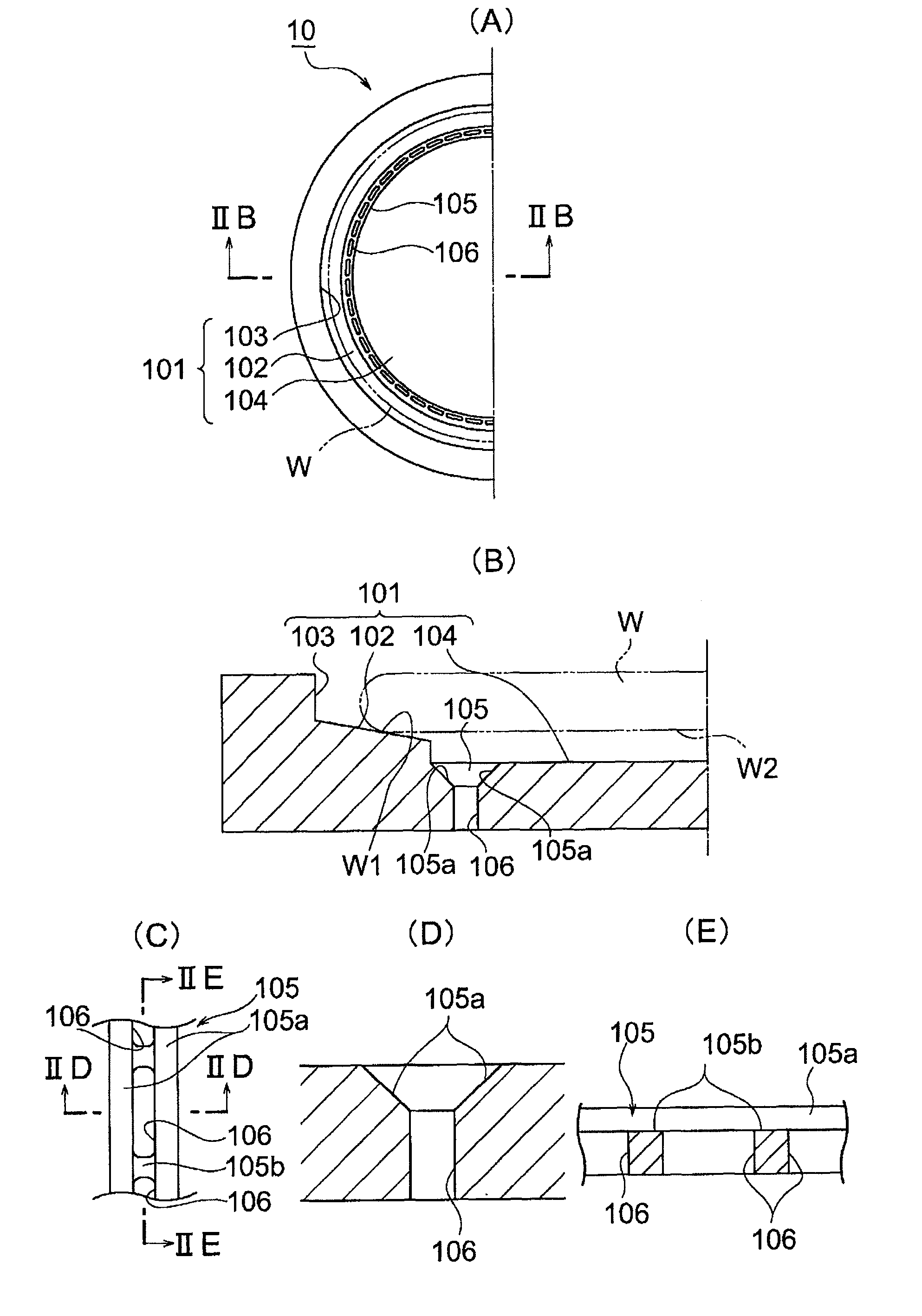
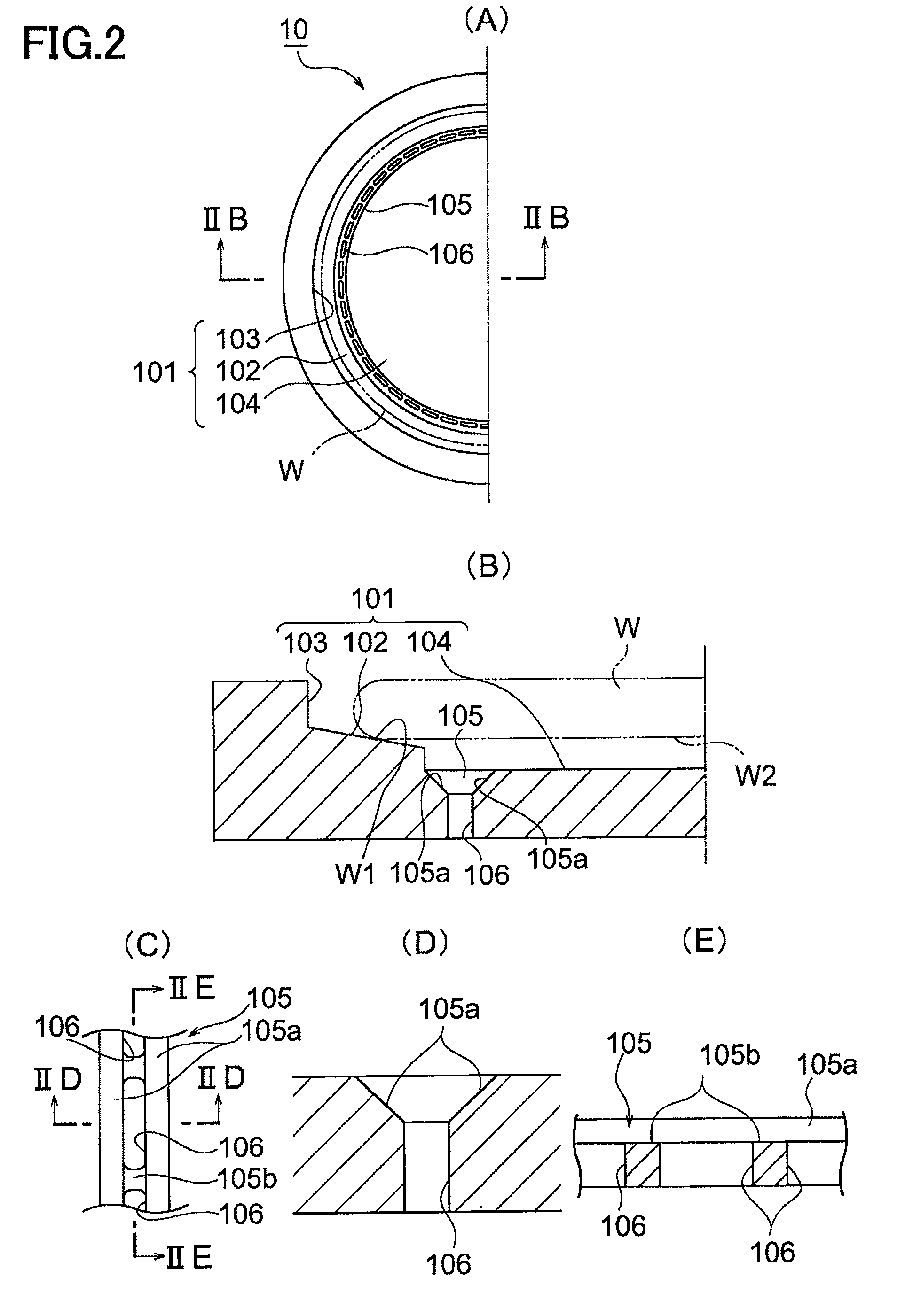
[0070]In a susceptor having the configuration as shown in FIG. 2, a diameter of the bottom surface was changed to 297 mm, a size of each gas release opening to 2.5 mm lengthwise×0.8 mm crosswise (opening area of 2.0 mm2), and the opening area ratio of the gas release openings to 0.25%, so that a silicon wafer having a diameter of 300 mm can be loaded.
[0071]The ring-shaped groove 105 was formed to be one row on the outermost circumference of the bottom surface 104, wherein the bottom portion 105b has two sloping planes 105a formed on both sides thereof and the gas release openings 106 were formed on the bottom surface of the ring-shaped groove 105 by the number of 130.
[0072]A hundred of silicon wafers having a diameter of 300 mm were loaded on the susceptor by supporting the lower surface of each wafer by pins and lowering the pins to place the wafer in the wafer pocket 101 from above the susceptor 10. An amount of deviation of the center of the wafer from the center of the wafer poc...
example 2
[0073]Other than changing the opening area ratio of the gas release openings to 0.5%, a susceptor was manufactured under the same condition as that in the example 1. Silicon wafers having a diameter of 300 mm were loaded on the susceptor by supporting the lower surface of each wafer by pins and lowering the pins to place the wafer in the wafer pocket 101 from above the susceptor 10. An amount of deviation of the center of the wafer from the center of the wafer pocket was measured.
example 3
[0074]Other than changing the opening area of each of the gas release openings to 3.0 mm2, a susceptor was manufactured under the same condition as that in the example 1. Silicon wafers having a diameter of 300 mm were loaded on the susceptor by supporting the lower surface of each wafer by pins and lowering the pins to place the wafer in the wafer pocket 101 from above the susceptor 10. An amount of deviation of the center of the wafer from the center of the wafer pocket was measured.
PUM
| Property | Measurement | Unit |
|---|---|---|
| area | aaaaa | aaaaa |
| diameter | aaaaa | aaaaa |
| diameter | aaaaa | aaaaa |
Abstract
Description
Claims
Application Information
 - R&D
- Intellectual Property
- Life Sciences
- Materials
- Tech Scout
- Unparalleled Data Quality
- Higher Quality Content
- 60% Fewer Hallucinations
Browse by: Latest US Patents, China's latest patents, Technical Efficacy Thesaurus, Application Domain, Technology Topic, Popular Technical Reports.
© 2025 PatSnap. All rights reserved.Legal|Privacy policy|Modern Slavery Act Transparency Statement|Sitemap|About US| Contact US: help@patsnap.com


