
Adaptive redundancy in three dimensional memory

a three-dimensional memory and redundancy technology, applied in error detection/correction, redundant data error correction, instruments, etc., can solve problems such as different error rates for data stored, and achieve the effect of higher expected error

Inactive Publication Date: 2015-04-21
SANDISK TECH LLC
View PDF19 Cites 64 Cited by
  • Summary
  • Abstract
  • Description
  • Claims
  • Application Information

AI Technical Summary

Benefits of technology

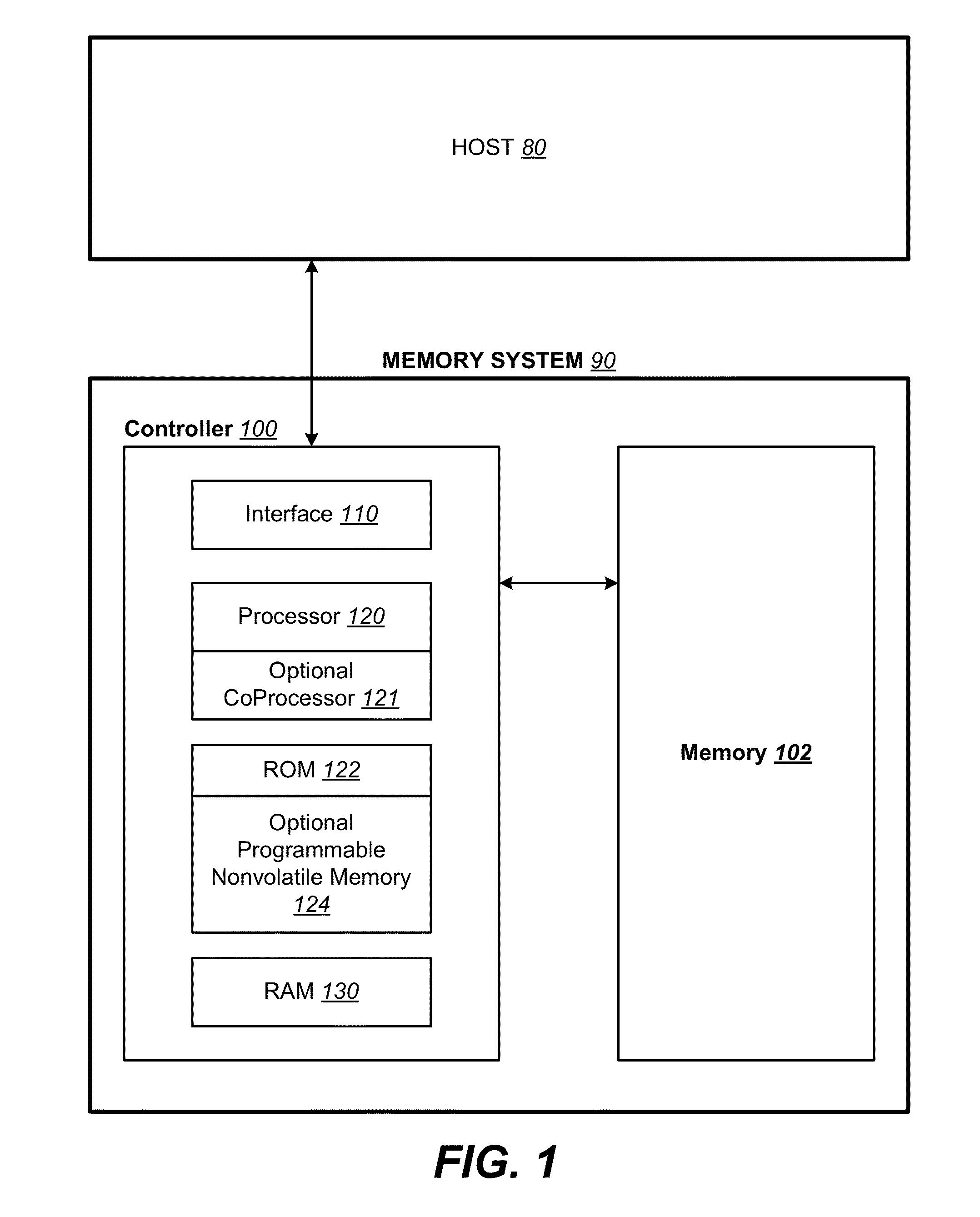
The patent describes a method and system for operating a three-dimensional nonvolatile memory that includes multiple physical levels of memory cells. The system categorizes the physical levels into high and low risk levels based on their expected error rates. It then performs a redundancy calculation for data in the high risk levels, storing the data in a redundant block in the memory. The system also includes a write circuit to regenerate the redundant data when it is identified as uncorrectable. The technical effect of this invention is to improve the reliability and performance of the three-dimensional nonvolatile memory, especially in the high risk physical levels where there are more bad bits.

Problems solved by technology

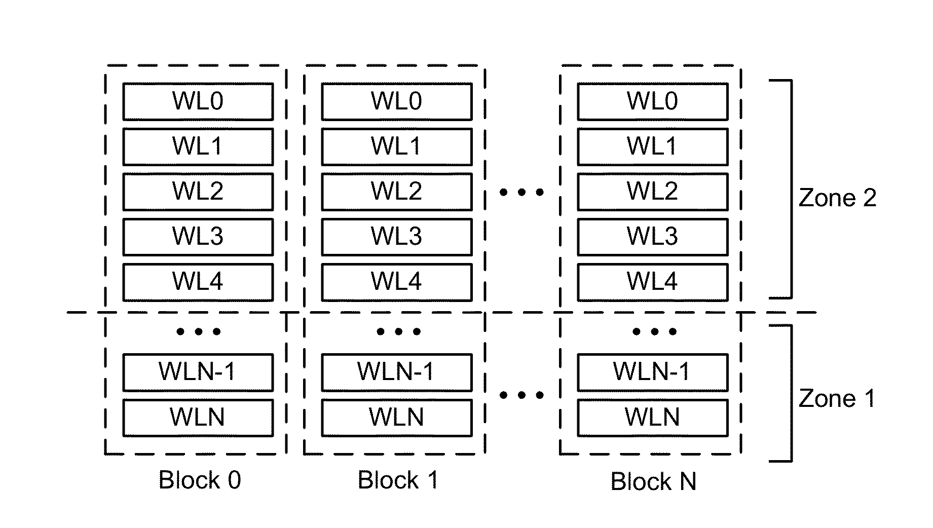
Such structures tend to be nonuniform from top to bottom, which tends to produce different error rates for data stored in different physical levels.

Method used


Image

  • Adaptive redundancy in three dimensional memory
  • Adaptive redundancy in three dimensional memory
  • Adaptive redundancy in three dimensional memory

Examples


Embodiment Construction

Memory System

[0038]Semiconductor memory devices include volatile memory devices, such as dynamic random access memory (“DRAM”) or static random access memory (“SRAM”) devices, non-volatile memory devices, such as resistive random access memory (“ReRAM”), electrically erasable programmable read only memory (“EEPROM”), flash memory (which can also be considered a subset of EEPROM), ferroelectric random access memory (“FRAM”), and magnetoresistive random access memory (“MRAM”), and other semiconductor elements capable of storing information. Each type of memory device may have different configurations. For example, flash memory devices may be configured in a NAND or a NOR configuration.

[0039]The memory devices can be formed from passive and / or active elements, in any combinations. By way of non-limiting example, passive semiconductor memory elements include ReRAM device elements, which in some embodiments include a resistivity switching storage element, such as an anti-fuse, phase chan...


PUM


Abstract

In a three-dimensional nonvolatile memory, physical layers are zoned according to expected error rate. Different redundancy schemes are applied to different zones so that a high degree of redundancy is applied to a zone with a high expected error rate and a low degree of redundancy is applied to a zone with a low expected error rate.

Description

BACKGROUND[0001]This application relates to the operation of re-programmable nonvolatile three dimensional memory such as semiconductor flash memory, resistive memory (e.g. ReRAM), and other memories formed in multiple physical layers.[0002]Solid-state memory capable of nonvolatile storage of charge, particularly in the form of EEPROM and flash EEPROM packaged as a small form factor card, has become the storage of choice in a variety of mobile and handheld devices, notably information appliances and consumer electronics products. Unlike RAM (random access memory) that is also solid-state memory, flash memory is non-volatile, and retains its stored data even after power is turned off. Also, unlike ROM (read only memory), flash memory is rewritable similar to a disk storage device.[0003]Flash EEPROM is similar to EEPROM (electrically erasable and programmable read-only memory) in that it is a non-volatile memory that can be erased and have new data written or “programmed” into their m...

Claims


Application Information

Patent Timeline
IPC IPC(8): G11C29/00G06F11/10
CPCG11C29/76G06F11/1076G11C16/0483G11C16/349G06F11/1048G06F11/108G11C29/028G11C29/56008G11C29/72
Inventor HU, XINDE
Owner SANDISK TECH LLC
Learn More