Photoelectric conversion element, light receiving device, light receiving system, and distance measuring device

a technology of photoelectric conversion and light receiving, which is applied in the direction of distance measurement, instruments, and using reradiation, etc., can solve the problems of time required for transferring to the output side all of the photoelectrons, the difference in the transfer efficiency between the two nodes, and the difficulty of photoelectrically converted photoelectrons to be transferred at high speeds. achieve the effect of improving the s/n ratio, reducing the influence of ambient light noise components, and high accuracy

Inactive Publication Date: 2015-02-03
HONDA MOTOR CO LTD
View PDF15 Cites 0 Cited by
  • Summary
  • Abstract
  • Description
  • Claims
  • Application Information

AI Technical Summary

Benefits of technology

[0009]The present invention has been made in consideration of the aforementioned problems, and has the object of providing a photoelectric conversion element in which photoelectrons obtained by photoelectric conversion can be transferred at high speeds to a desired region and accumulated therein, in which a distance measuring device can be realized by applying the principles of a TOF method, and which further enables the invention to be applied to various light receiving devices.
[0047]Still further, according to the distance measuring device of the present invention, the S / N ratio can be improved, the influence of ambient light noise components can be reduced, and the distance to an object can be measured with high accuracy.

Problems solved by technology

Accordingly, a problem occurs in that time is required for transferring to the output side all of the photoelectrons stored in the light-receiving element.
However, in the case of using a large photoelectric conversion element, the distance to the output node is long, and hence it is difficult for the photoelectrically converted photoelectrons to be transferred at high speeds to a desired node.
Furthermore, in the case that photoelectrons are allocated to two nodes from the photoelectric conversion element, if the distances to respective gate electrodes from the photoelectric conversion element are different, then a difference in the transfer efficiency to the two nodes occurs, which results in lowering of the S / N ratio, caused by the existence of an in-plane distribution in the conversion efficiency of the photoelectric conversion element, or differences in the transfer paths of the photoelectrons.

Method used


Image

  • Photoelectric conversion element, light receiving device, light receiving system, and distance measuring device
  • Photoelectric conversion element, light receiving device, light receiving system, and distance measuring device
  • Photoelectric conversion element, light receiving device, light receiving system, and distance measuring device

Examples


first embodiment

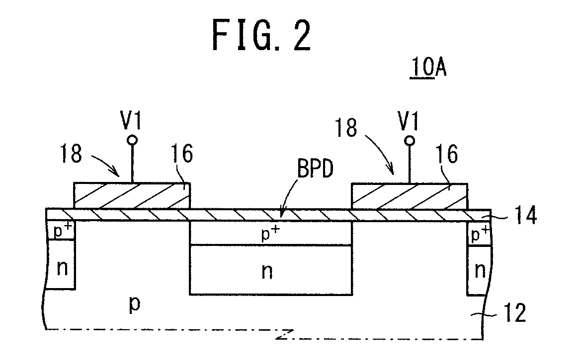
[0096]First, as shown in FIGS. 1 and 2, a photoelectric conversion element (hereinafter referred to as a first photoelectric conversion element 10A) according to the present invention includes one MOS diode 18 having an electrode 16 formed on a semiconductor substrate (see FIG. 2) with an insulator 14 disposed therebetween, and embedded photodiodes BPD formed on the semiconductor substrate 12. More specifically, as shown in FIG. 2, for example, the semiconductor substrate 12 is formed by a p-type impurity diffusion region. Additionally, the aforementioned MOS diode 18 is made by forming the electrode 16 from polysilicon or a metallic conductor or the like on the semiconductor substrate 12 via an insulator layer (insulator 14) made from SiO2 or the like. Further, the aforementioned embedded photodiodes BPD are constituted respectively by forming a high density p-type impurity diffusion region on the surface of an n-type impurity diffusion region, which itself is formed on a p-type im...

second embodiment

[0107]Next, a photoelectric conversion element (hereinafter referred to as a second photoelectric conversion element 10B) according to the present invention shall be described with reference to FIGS. 6 through 9.

[0108]As shown in FIG. 6, the second photoelectric conversion element 10B includes roughly the same structure as the aforementioned first photoelectric conversion element 10A, however, the second photoelectric conversion element 10B includes one first MOS diode 18a having a first electrode 16a, which is formed on the semiconductor substrate (see FIG. 7) with an insulator 14 disposed therebetween, and plural second MOS diodes 18b having second electrodes 16b, which are formed on the semiconductor substrate 12 with the insulator 14 disposed therebetween. The first MOS diode 18a is constituted the same as the MOS diode 18 of the aforementioned first photoelectric conversion element 10A. More specifically, for example as shown in FIG. 7, the semiconductor substrate 12 is formed ...

third embodiment

[0294]As shown in FIG. 29, a photoelectric conversion element (hereinafter referred to as a third photoelectric conversion element 10C) has substantially the same structure as the aforementioned second photoelectric conversion element 10B, except that the shapes of the first electrode 16a and the second electrodes 16b are different, in particular, as viewed from the upper surface thereof.

[0295]More specifically, each of the branch portions 22 of the first electrode 16a has a shape such that the electrode width thereof gradually widens toward the one electrode portion 20 as viewed from the upper surface, and each of the second electrodes has a shape such that the electrode width thereof gradually narrows toward the one electrode portion 20 as viewed from the upper surface.

[0296]In the case that a potential location 32a beneath the one electrode 16a is focused on and viewed, as shown in FIGS. 30A and 30B, the portion thereof where the electrode width is narrow receives an influence f...


PUM


Abstract

A first photoelectric conversion element, which detects light and converts the light into photoelectrons has: one MOS diode having an electrode formed on a semiconductor base body with an insulator therebetween; and a plurality of embedded photodiodes formed in the semiconductor base body. The electrode of the MOS diode has, when viewed from the upper surface, a comb-like shape wherein a plurality of branch portions are branched from one electrode portion. Each of the embedded photodiodes is disposed to nest between the branch portions of the electrode when viewed from the upper surface.

Description

TECHNICAL FIELD[0001]The present invention relates to a photoelectric conversion element that converts light into an electric charge corresponding to the light amount thereof, a light receiving device that acquires luminance information of incident light to the photoelectric conversion element in a fixed time period, a light receiving system in which the influence of ambient light is controlled using the photoelectric conversion element, and a distance measuring device in which the principles of a time-of-flight (TOF) method are applied using the light receiving system.BACKGROUND ART[0002]Heretofore, an image sensor has been proposed, which is capable of signal detection at a high S / N ratio while removing the influence of ambient light (see, Koji Yamamoto, “Furiwake Tenso Hoshiki Oyobi Bubun Ryoiki Kosoku Yomidashi Hoshiki ni yoru Hencho Hikari Seibun Kenshutsu Kano na CMOS Image Sensor ni Kansuru Kenkyu (Research in Relation to CMOS Image Sensors Capable of Modulated Light Componen...

Claims


Application Information

Patent Timeline
Patent Type & Authority Patents(United States)
IPC IPC(8): G01C3/08G01B11/02G01S7/4863G01S17/894
CPCG01B11/026G01S7/4863G01S17/89G01S17/894
Inventor KAMIYAMA, TOMOYUKIKOREKADO, KEISUKE
Owner HONDA MOTOR CO LTD
Why Eureka
Try Eureka