Power transfer system and noncontact charging device
a technology of power transmission system and charging device, which is applied in the direction of electrical apparatus construction details, transportation and packaging, inductance, etc., can solve the problems of unnecessary electric field, increased voltage applied to each electrode, and reduced flexibility of arrangement of both power transmission device and power reception devi
- Summary
- Abstract
- Description
- Claims
- Application Information
AI Technical Summary
Benefits of technology
Problems solved by technology
Method used
Image
Examples
first embodiment
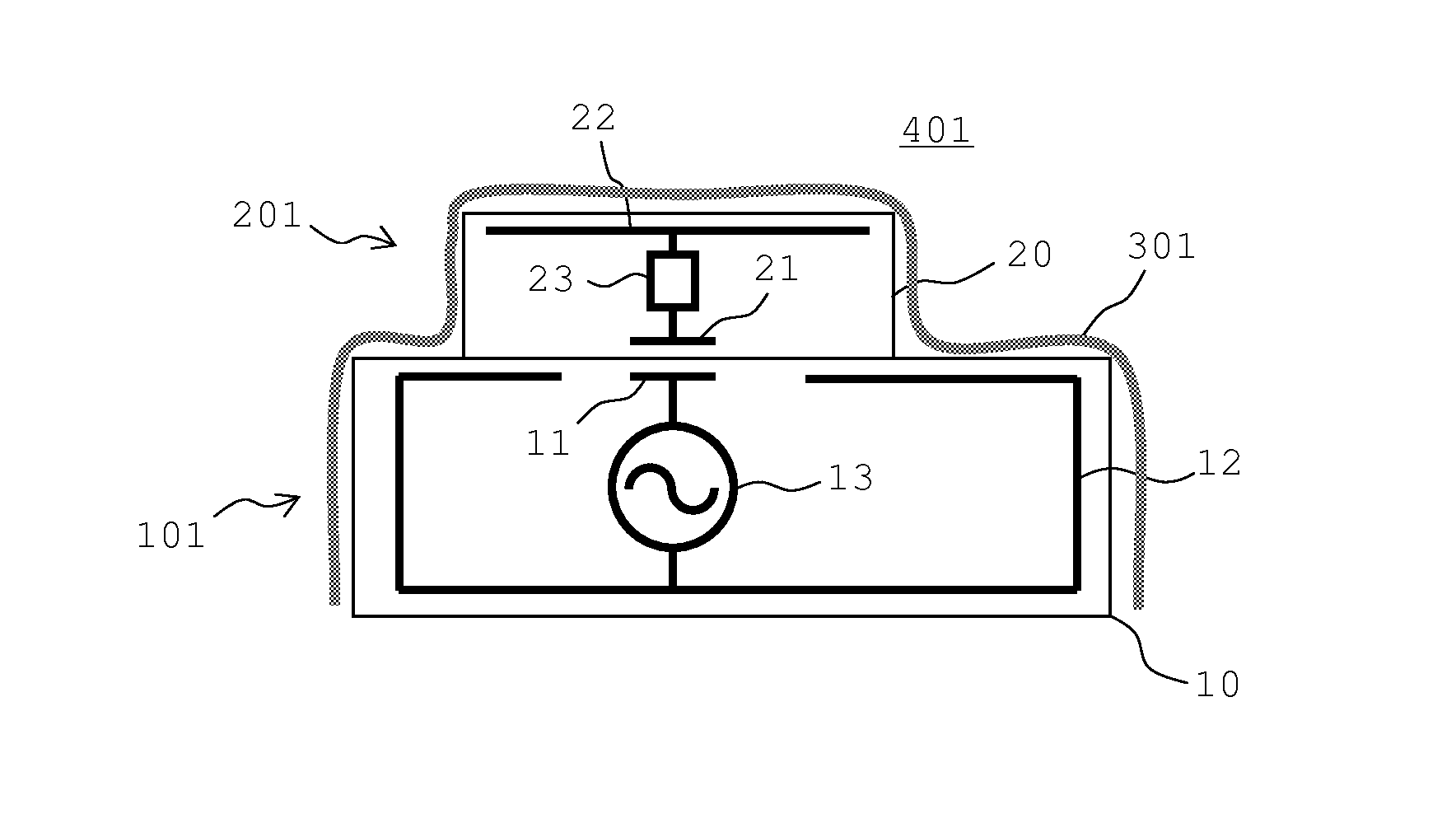
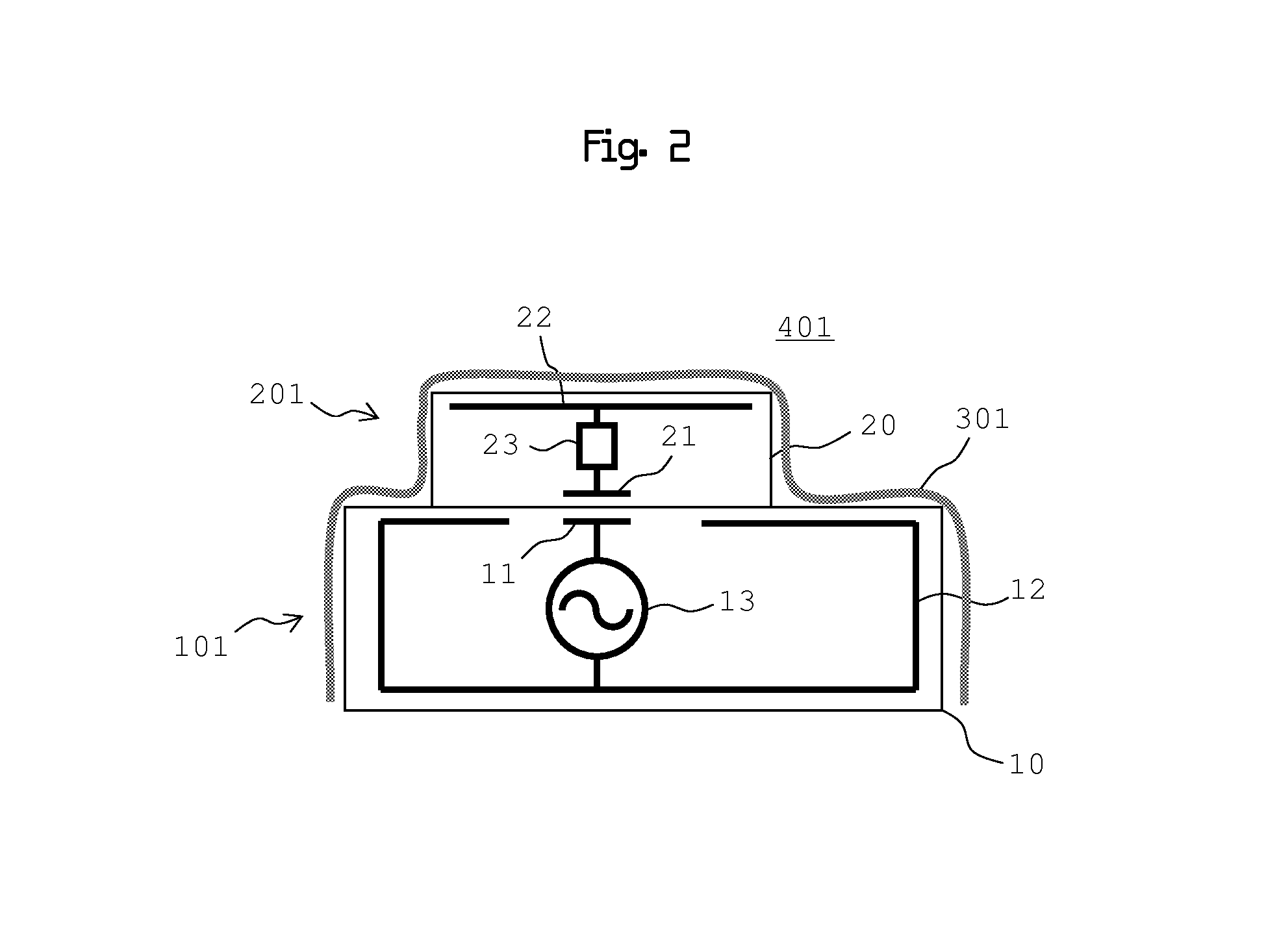
[0026]The configuration of a power transfer system according to a first embodiment will be described with reference to FIG. 2 to FIG. 4. FIG. 2 is a cross-sectional view that conceptually shows a relevant portion of a power transfer system 401. The power transfer system 401 includes a power transmission device 101 and a power reception device 201. A high-voltage side conductor 11 and a low-voltage side conductor 12 are formed near the upper surface of a casing 10 of the power transmission device 101. The low-voltage side conductor 12 surrounds the high-voltage side conductor 11 in an insulated state from the high-voltage side conductor 11. In addition, an alternating voltage generating circuit 13 is provided inside the casing 10 of the power transmission device 101 and applies an alternating voltage between the high-voltage side conductor 11 and the low-voltage side conductor 12. In this example, the low-voltage side conductor 12 is arranged along the outer peripheral surface of the...
second embodiment
[0046]FIG. 5 is a cross-sectional view that conceptually shows a relevant portion of a power transfer system 402 according to a second embodiment. The power transfer system 402 includes a power transmission device 102 and a power reception device 202.
[0047]In the example shown in FIG. 2, the power reception device 201 is placed on the power transmission device 101. FIG. 5 shows an example in which the power transmission device 102 and the power reception device 202 are arranged side by side. As shown in FIG. 5, a high-voltage side conductor 11 is provided at the side of the power transmission device 102, a high-voltage side conductor 21 is provided at the side of the power reception device 202, and a capacitive coupling conductor 302 covers the power transmission device 102 and the power reception device 202 that are arranged side by side. In this manner, it is possible to achieve capacitive coupling.
third embodiment
[0048]FIG. 6 is a cross-sectional view that conceptually shows a relevant portion of a power transfer system 403 according to a third embodiment. The configuration of the power transfer system 403 differs from that shown in FIG. 2 in that the capacitive coupling conductor 302 is electrically continuous with the low-voltage side conductor 12 of the power transmission device 103. With the above configuration, a capacitance generated between the capacitive coupling conductor 302 and the low-voltage side conductor 22 is directly connected between the low-voltage side conductors 12 and 22. Thus, it is possible to increase (gain) a capacitance between the low-voltage side conductors 12 and 22.
PUM
 Abstract
Description
Claims
Application Information
 - R&D
- Intellectual Property
- Life Sciences
- Materials
- Tech Scout
- Unparalleled Data Quality
- Higher Quality Content
- 60% Fewer Hallucinations
Browse by: Latest US Patents, China's latest patents, Technical Efficacy Thesaurus, Application Domain, Technology Topic, Popular Technical Reports.
© 2025 PatSnap. All rights reserved.Legal|Privacy policy|Modern Slavery Act Transparency Statement|Sitemap|About US| Contact US: help@patsnap.com


