Power transfer system and noncontact charging device
a technology of power transmission system and charging device, which is applied in the direction of battery data exchange, inductance, electrical apparatus construction details, etc., can solve the problems of unnecessary electric field, increased voltage applied to each electrode, and reduced flexibility of arrangement of both power transmission device and power reception devi
- Summary
- Abstract
- Description
- Claims
- Application Information
AI Technical Summary
Benefits of technology
Problems solved by technology
Method used
Image
Examples
first embodiment
[First Embodiment]
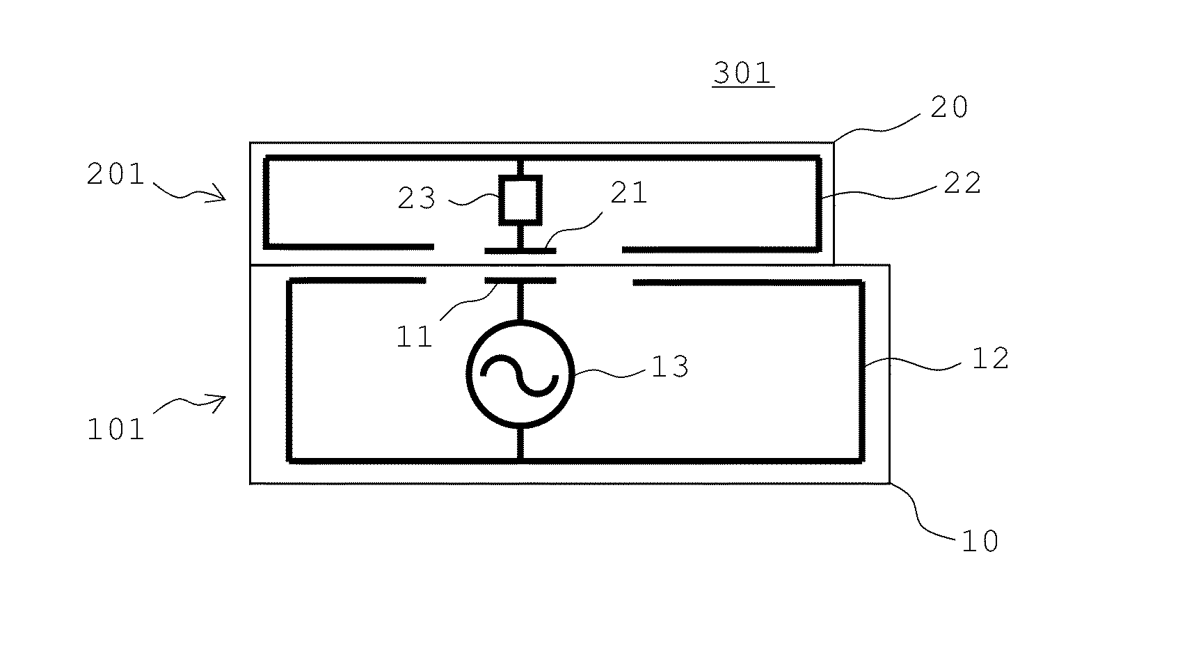
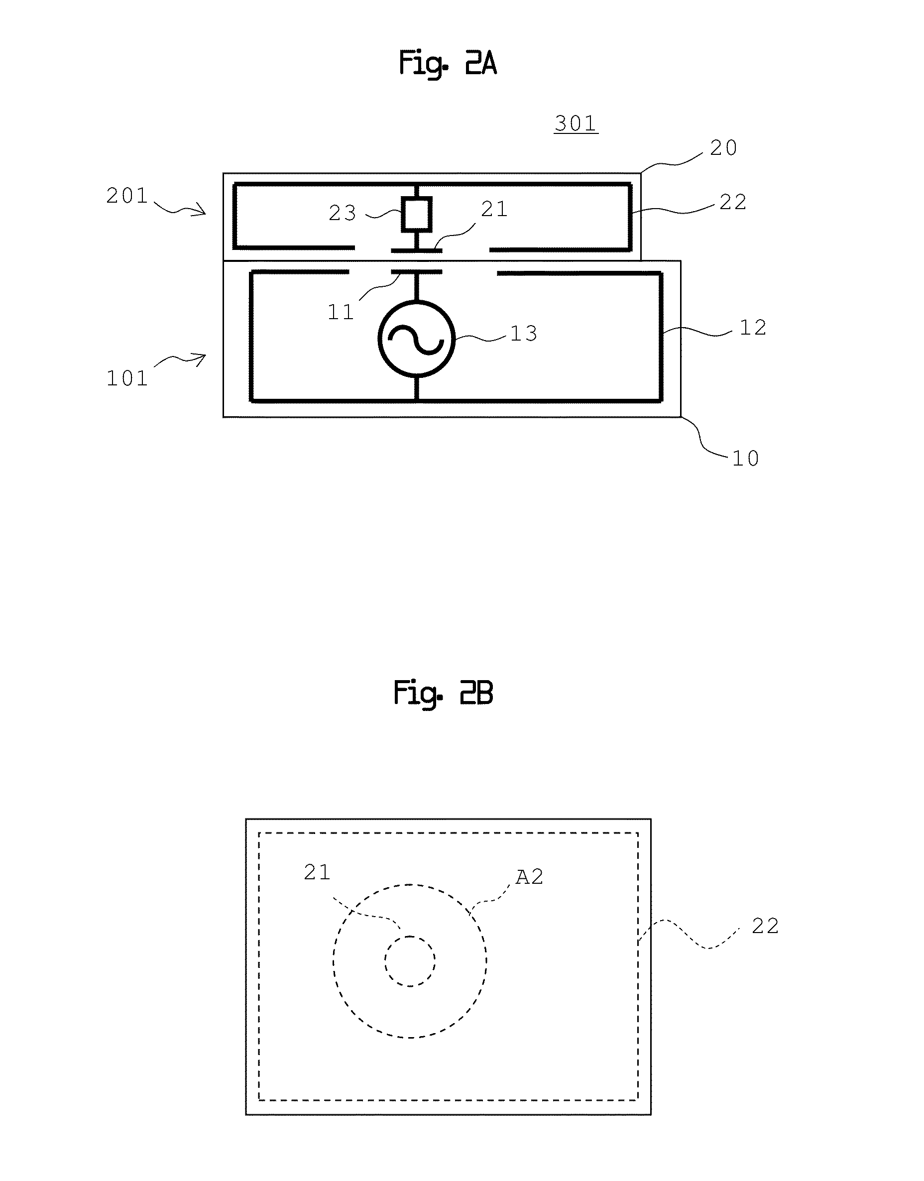
[0056]The configuration of a power transfer system according to a first embodiment will be described with reference to FIG. 2A to FIG. 4. FIG. 2A is a cross-sectional view that conceptually shows a relevant portion of a power transfer system 301. The power transfer system 301 includes a power transmission device 101 and a power reception device 201. A central conductor 11 and a peripheral conductor 12 are formed near the upper surface of a casing 10 of the power transmission device 101. The peripheral conductor 12 surrounds the central conductor 11 in an insulated state from the central conductor 11. In addition, an alternating voltage generating circuit 13 is provided inside the casing 10 of the power transmission device 101 and applies an alternating voltage between the central conductor 11 and the peripheral conductor 12. In this example, the peripheral conductor 12 is arranged along the outer peripheral surface of the casing 10. Thus, the alternating voltage ge...
second embodiment
[Second Embodiment]
[0080]FIG. 5 is a cross-sectional view that conceptually shows a relevant portion of a power transfer system 302 according to a second embodiment. The power transfer system 302 includes a power transmission device 101 and a power reception device 204.
[0081]The configuration of the power transmission device 101 is similar to that of the power transmission device 101 shown in FIG. 2A, and includes a central conductor 11, a peripheral conductor 12 and an alternating voltage generating circuit 13 inside a casing 10.
[0082]On the other hand, the power reception device 204 includes a central conductor 21, a metal casing 24 and a load circuit 23. The power reception device 204 differs from the power reception device 201 shown in FIG. 2A in that a metal casing 24 of the power reception device 204 shown in FIG. 5A also serves as a peripheral conductor. The central conductor 21 is arranged so that the central conductor 21 is not exposed to an outer surface in an insulated st...
third embodiment
[Third Embodiment]
[0088]FIG. 7A to FIG. 7D are views that show the configurations of four power transfer systems 303, 304, 305, and 306 according to a third embodiment. The power transfer system 303 shown in FIG. 7A includes a power transmission device 104 and a power reception device 205. As in the case of the examples shown in the first and second embodiments, the power transmission device 104 includes a central conductor 11, a peripheral conductor 12 and an alternating voltage generating circuit 13 inside a casing 10. In addition, the power reception device 205 includes a central conductor 21, a peripheral conductor 22 and a load circuit 23 inside a casing 20. A convex portion 10S is formed on the active surface of the casing 10 of the power transmission device 104. A concave portion 20D is formed on the active surface of the casing 20 of the power reception device 205.
[0089]The convex portion 10S and the concave portion 20D are formed so that the central conductor 11 of a power ...
PUM
| Property | Measurement | Unit |
|---|---|---|
| frequency | aaaaa | aaaaa |
| voltage | aaaaa | aaaaa |
| frequency | aaaaa | aaaaa |
Abstract
Description
Claims
Application Information
 - R&D
- Intellectual Property
- Life Sciences
- Materials
- Tech Scout
- Unparalleled Data Quality
- Higher Quality Content
- 60% Fewer Hallucinations
Browse by: Latest US Patents, China's latest patents, Technical Efficacy Thesaurus, Application Domain, Technology Topic, Popular Technical Reports.
© 2025 PatSnap. All rights reserved.Legal|Privacy policy|Modern Slavery Act Transparency Statement|Sitemap|About US| Contact US: help@patsnap.com


