Dual polarization optical modulator using dual broadband multi-electrode weighted direct analog phase modulators
a dual-polarization, analog phase modulator technology, applied in optics, instruments, optical light guides, etc., can solve the problems of low modulation efficiency per unit length, degrade the quality of constellation diagrams, and mismatch in frequency respons
- Summary
- Abstract
- Description
- Claims
- Application Information
AI Technical Summary
Benefits of technology
Problems solved by technology
Method used
Image

Examples
first embodiment
[0043]FIG. 5 illustrates the present disclosure comprising a three interaction section modulator from two staggered electrodes. RF signal electrode #1 206 has two interaction regions 206a that are before and after a single interaction region 208a for RF signal electrode #2 208. The sum of the first and third interaction regions, L1+L3, is twice that of the second interaction region of length L2 in order to achieve the 2:1 scaling ratio of modulation strengths. The third interaction region length, L3, is longer than the first, L1, to compensate for RF loss in the electrode. The difference in lengths of the first and third sections causes the center of the second section to be before the center of the entire structure. The lengths of the three sections, L1, L2, and L3, normalized to the total electrode length, are 0.309, 0.333, and 0.358, respectively. For this design, the I signal is applied to signal electrode #1 while the Q signal is applied to signal electrode #2.
[0044]In FIG. 5, ...
third embodiment
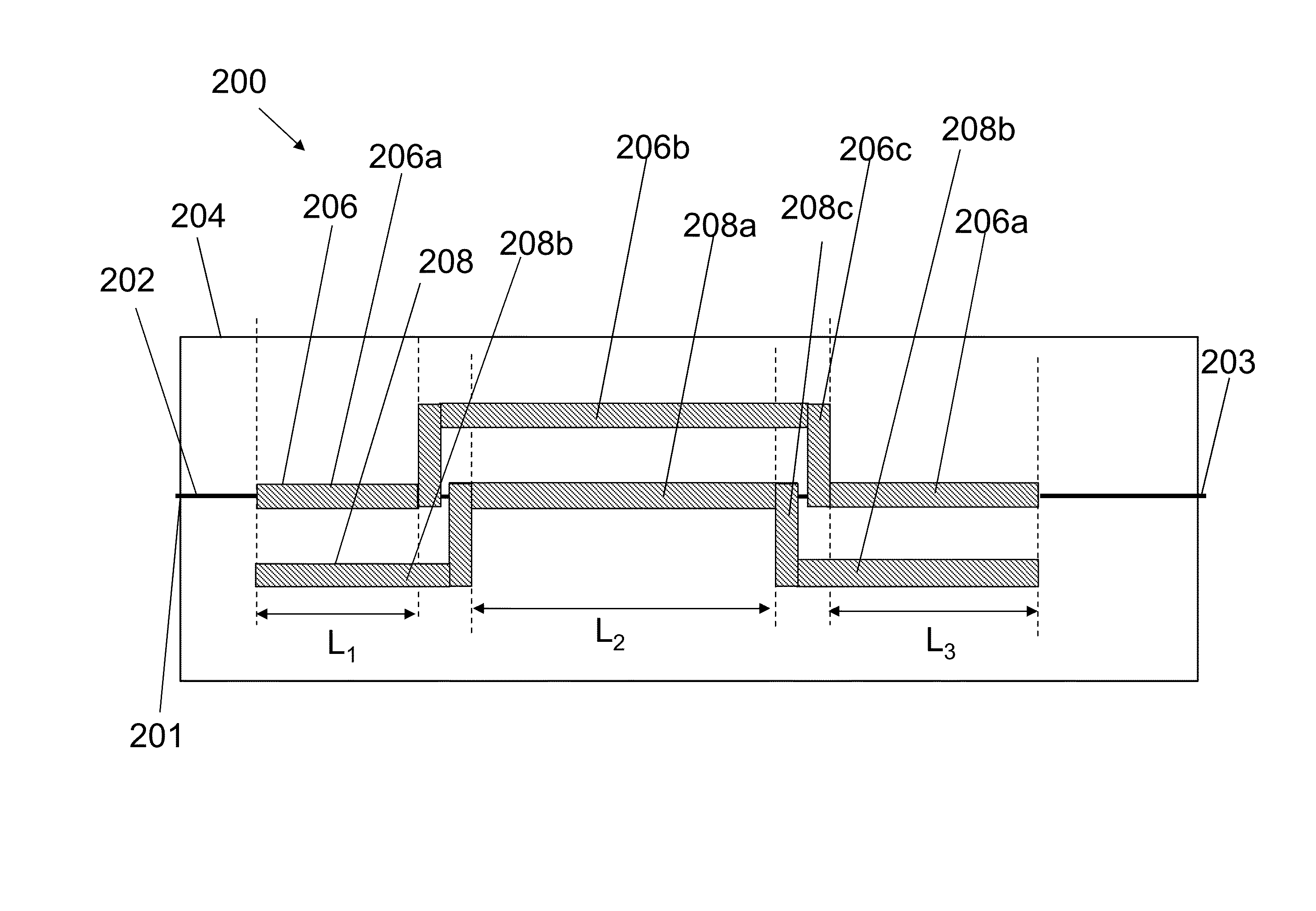
[0053]FIG. 11 illustrates the present disclosure where a six section modulator is formed from three staggered electrodes. An electro-optical phase modulator 400 comprises a waveguide 402 having an input end 401 and an output end 403 is formed in a single domain structure electro-optical substrate 404. Three signal electrodes 406,408 and 410 are provided on the substrate 404 forming shifting lines along the waveguide 402 from a first end proximate to the input 401 to a second end proximate to the output 403. Between the ends of each electrode 406, 408, 410 are a plurality of interaction lengths, shifted lengths and transition lengths. Using electrode 406 as an example, two interaction lengths 406a and four shifted lengths 406b are interspaced by five transition lengths 406c. The electrodes 406, 408 and 410 have a complimentary cascading structure that allows each of the three electrodes 406, 408, 410 to transition between interaction regions and alternate which electrode 406, 408, 41...
embodiment 500
[0091]FIG. 20 provides an enlarged view of an interaction region of the embodiment 500′ of FIG. 19. Specifically, interaction region IR1 of modulator 502 is illustrated in greater detail. As described in U.S. Pat. No. 7,701,630, the interaction region IR1 includes an interaction length that is split into several sections that alternate between modulating different waveguides with a pair of electrode polarity and domain inversion sections INVa and INVb. The interaction length 601 is divided into four sections 602, 604, 606 and 608. Sections 602 and 606 have unequal length and modulate the same waveguide branch 610. Sections 606 and 608 have unequal length and modulate the same waveguide branch 612. Transition sections 614 within the interaction length 601 displace the signal electrode between waveguide branches 610, 612.
[0092]Although the waveguides and electrode structures have been illustrated as straight lined structures, in some embodiments the waveguides and electrode structures...
PUM
 Abstract
Description
Claims
Application Information
 - R&D
- Intellectual Property
- Life Sciences
- Materials
- Tech Scout
- Unparalleled Data Quality
- Higher Quality Content
- 60% Fewer Hallucinations
Browse by: Latest US Patents, China's latest patents, Technical Efficacy Thesaurus, Application Domain, Technology Topic, Popular Technical Reports.
© 2025 PatSnap. All rights reserved.Legal|Privacy policy|Modern Slavery Act Transparency Statement|Sitemap|About US| Contact US: help@patsnap.com