Metal alloy with an abrupt interface to III-V semiconductor
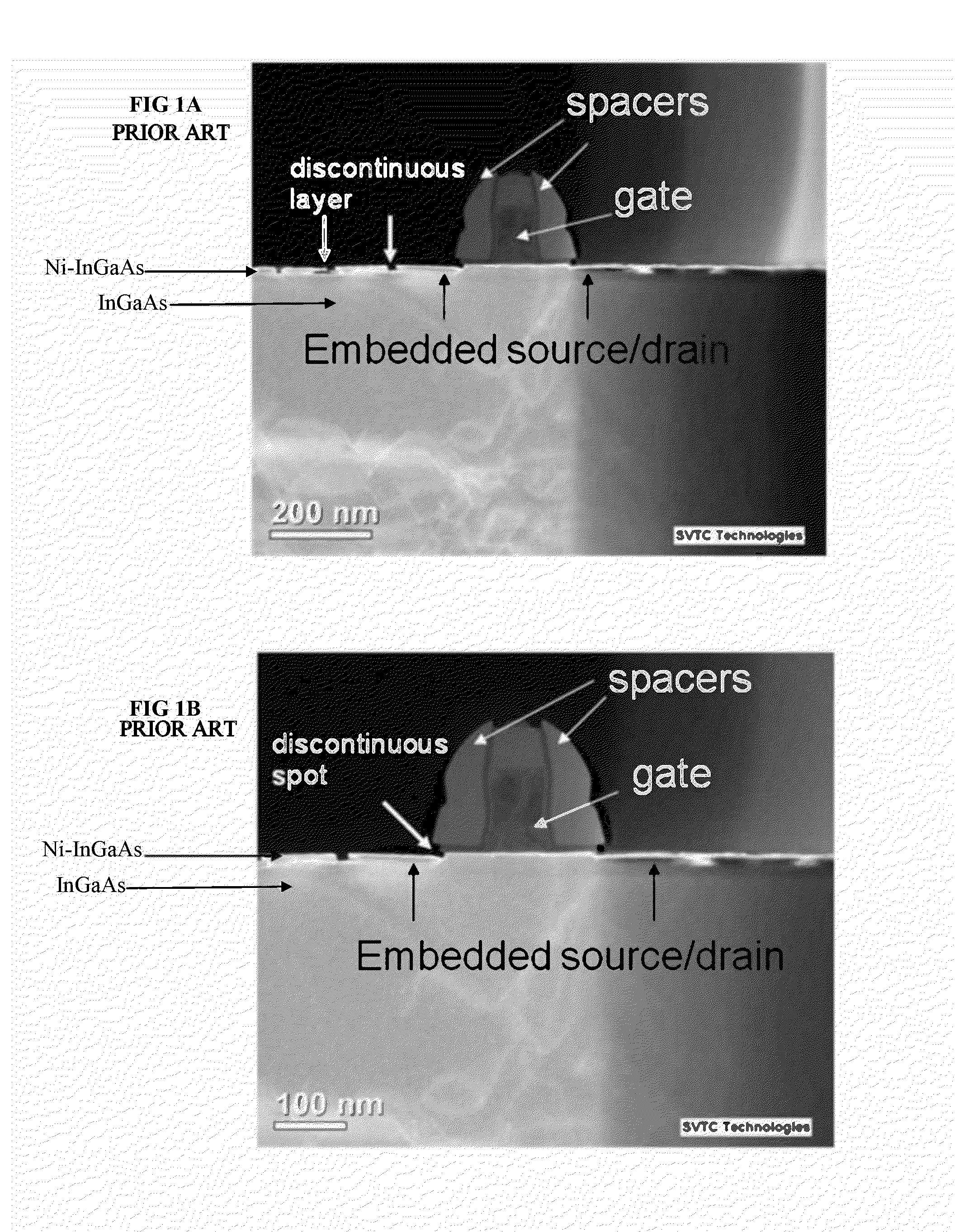
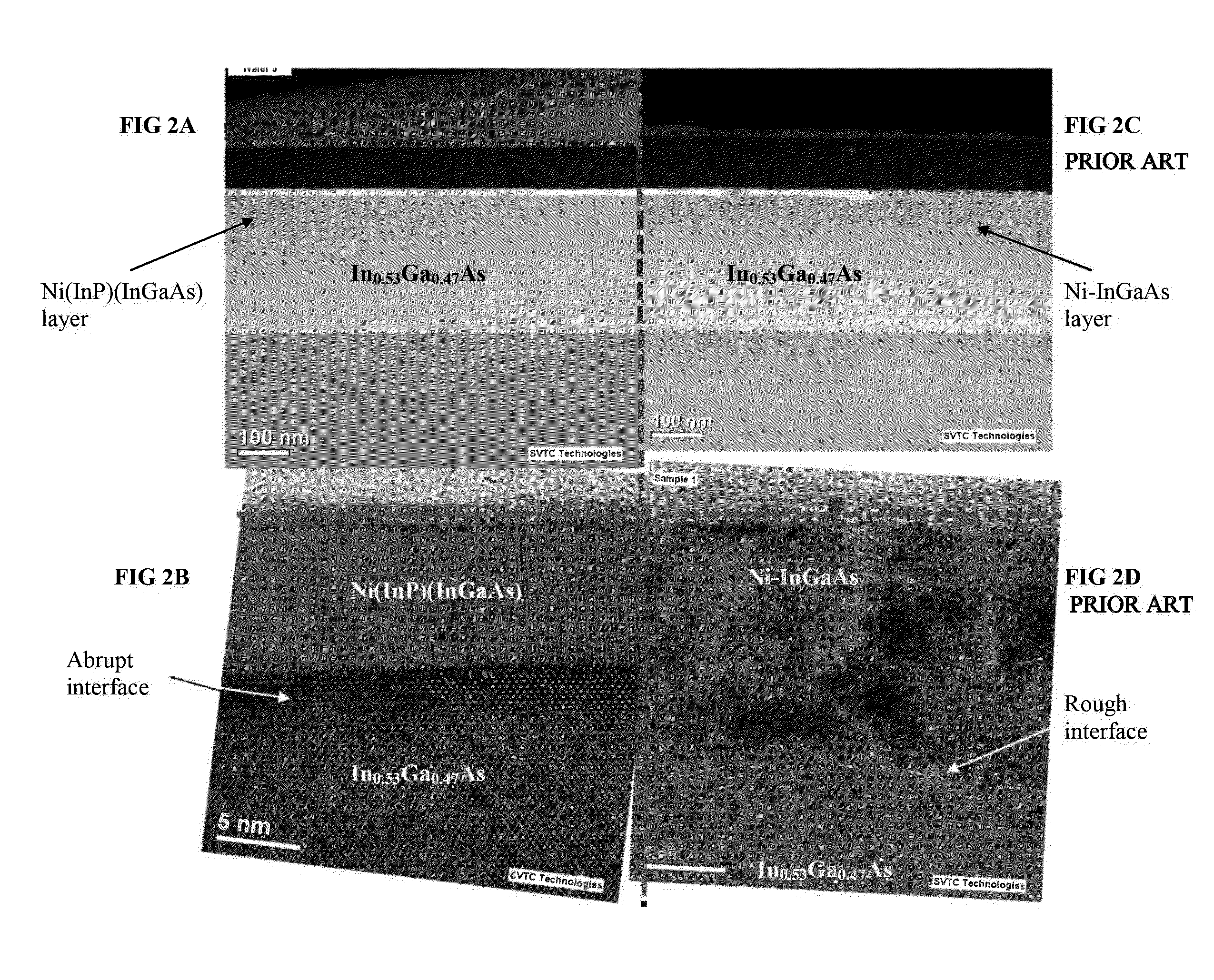
a metal alloy and abrupt interface technology, applied in the field of metal alloys with abrupt interfaces, can solve problems such as degrading device performance, and achieve the effects of reducing interface roughness and/or sheet resistance (sheet resistivity), reducing leakage current and/or contact resistance (rc), and reducing interface roughness
- Summary
- Abstract
- Description
- Claims
- Application Information
AI Technical Summary
Problems solved by technology
Method used
Image
Examples
examples b
, C, D, E, and F
[0058]Examples B, C, D, E, and F were prepared using the same process as described in Example A, except different annealing temperatures (250° C., 300° C., 350° C., 450° C., and 500° C., respectively) were used to form the Ni(InP)(InGaAs) alloy.
[0059]Counterexamples B2, C2, D2, E2, and F2.
[0060]Counterexamples B2, C2, D2, E2, and F2 were prepared using the same process as for Counterexample A2, except different annealing temperatures (250° C., 300° C., 350° C., 450° C., and 500° C., respectively) were used to form the Ni—InGaAs alloy.
[0061]FIG. 4 is a plot showing comparative sheet resistivity (Rsheet) values for Examples A-F according to the present invention (fabricated with an InP interlayer) versus Counterexamples A2-F2 (fabricated without an InP interlayer). As is evident from FIG. 4, the metal(III-V) alloys formed with a 5 nm InP layer all had comparable Rsheet values to that of metal(III-V) alloys formed on InGaAs without an InP interlayer. However, at tempera...
examples g
and H
[0062]Examples G and H were prepared using the same process as described in Example A, except that 10 nm and 15 nm of Ni, respectively for Example G and Example H, were deposited instead of 5 nm of Ni.
[0063]FIGS. 5A-D are XTEM micrograph images of metal / III-V interfaces in semiconductor structures. FIG. 5A corresponds to the semiconductor structure of Example A, whereas FIGS. 5B and 5C correspond to Example G and Example H, respectively. FIG. 5D is an image of a portion of the semiconductor structure fabricated in Counterexample A2. FIGS. 5A-C demonstrate that the metal / III-V interface remained smooth even at a metal(InP)(III-V) alloy thickness of 28 nm, which is considerably thicker than the 5 nm InP interlayer thickness. FIG. 5D demonstrates that even at a Ni thickness of 5 nm, the metal / III-V interface of the semiconductor structure fabricated without an InP layer is non-planar with significant variations in the alloy thickness (14-23 nm).
PUM
| Property | Measurement | Unit |
|---|---|---|
| thick | aaaaa | aaaaa |
| thick | aaaaa | aaaaa |
| temperature | aaaaa | aaaaa |
Abstract
Description
Claims
Application Information
 - R&D
- Intellectual Property
- Life Sciences
- Materials
- Tech Scout
- Unparalleled Data Quality
- Higher Quality Content
- 60% Fewer Hallucinations
Browse by: Latest US Patents, China's latest patents, Technical Efficacy Thesaurus, Application Domain, Technology Topic, Popular Technical Reports.
© 2025 PatSnap. All rights reserved.Legal|Privacy policy|Modern Slavery Act Transparency Statement|Sitemap|About US| Contact US: help@patsnap.com


