Eureka AIR delivers breakthrough ideas for toughest innovation challenges, trusted by R&D personnel around the world.

Semiconductor pressure sensor

a technology of semiconductors and sensors, applied in the direction of fluid pressure measurement, acceleration measurement using interia forces, instruments, etc., can solve the problems of manufacturing costs, increasing the size of sensors, increasing the number of manufacturing processes, etc., to improve the offset drift and offset voltage of the wheatstone bridge circuit, the effect of simplifying the manufacturing process

Active Publication Date: 2014-08-19
PANASONIC CORP
View PDF22 Cites 5 Cited by
  • Summary
  • Abstract
  • Description
  • Claims
  • Application Information

AI Technical Summary

Benefits of technology

[0011]In view of the above, the present invention provides a semiconductor pressure sensor capable of achieving miniaturization of a configuration and simplification of a manufacturing process.
[0012]Further, the present invention also provides the semiconductor pressure sensor capable of improving an offset voltage and offset drift of a Wheatstone bridge circuit composed of piezoresistive elements.
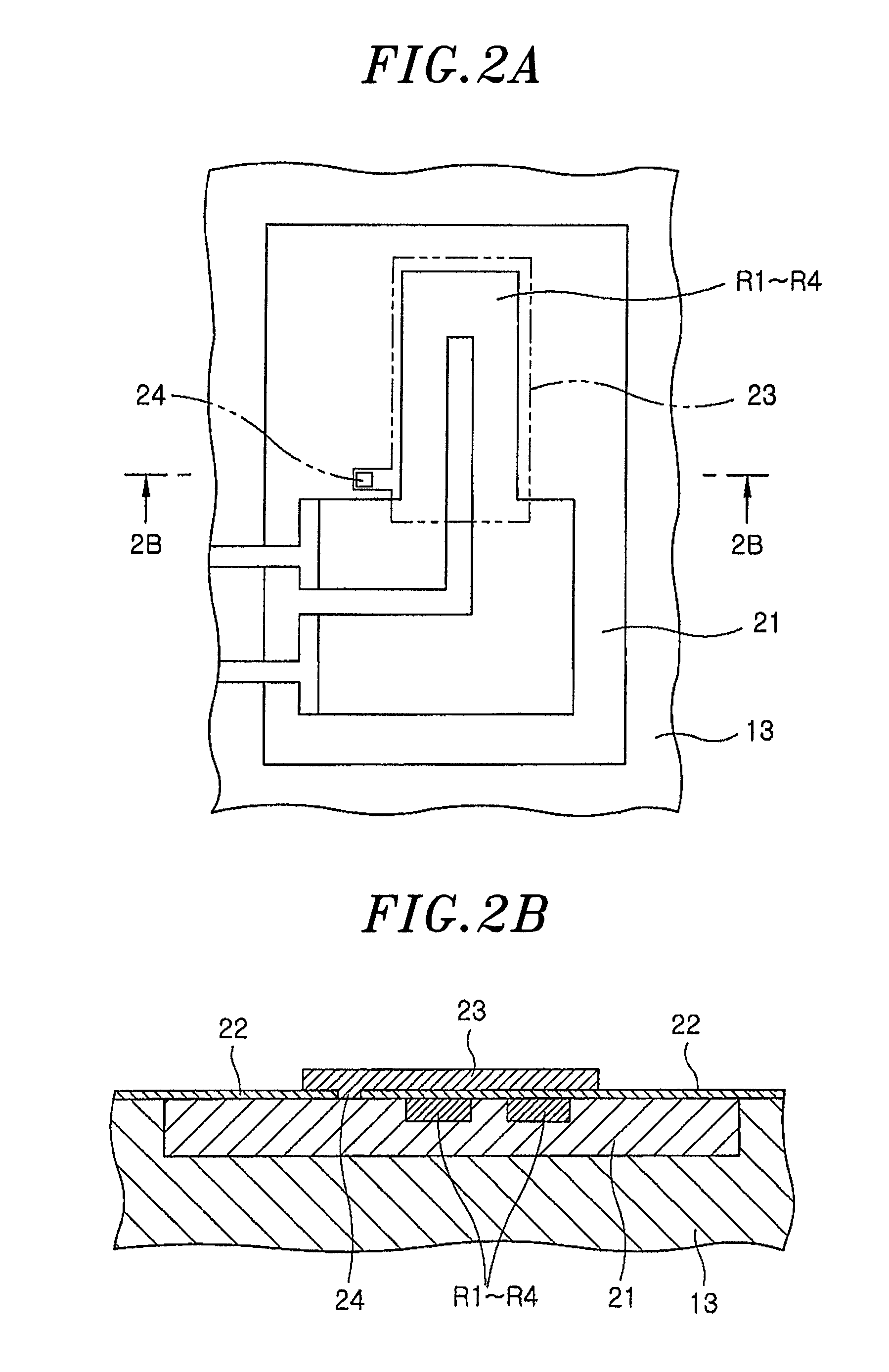
[0015]In accordance with the present invention, since the n-type semiconductor region and the shielding thin film layer, which is formed on the piezoresistive element formed in the corresponding n-type semiconductor region, are electrically connected to each other in the diaphragm, it is possible to apply a predetermined potential to the shielding thin film layer through the n-type semiconductor region. Thus, a wiring for applying a predetermined potential to the shielding thin film layer is not required, and it is possible to achieve miniaturization of the configuration and simplification of the manufacturing process.
[0016]Further, in accordance with the present invention, the shielding thin film layers, which are formed on the piezoresistive elements connected to the high voltage of the Wheatstone bridge circuit, are electrically connected to each other, and the shielding thin film layers, which are formed on the piezoresistive elements connected to the low voltage of the Wheatstone bridge circuit, are electrically connected to each other. Accordingly, the shielding thin film layers, which are formed on the piezoresistive elements connected to the high voltage of the Wheatstone bridge circuit, and the shielding thin film layers, which are formed on the piezoresistive elements connected to the low voltage of the Wheatstone bridge circuit, can be fixed at different potentials. As a result, it is possible to substantially equalize the degree of electrical influence on each of the piezoresistive elements from the corresponding shielding thin film layer, and it is possible to improve the offset drift and offset voltage of the Wheatstone bridge circuit.

Problems solved by technology

Accordingly, it leads to a problem such that the configuration of the sensor becomes large in size and the product cost increases.
Further, it becomes necessary to provide the connection film for connecting the shield thin film to the substrate potential, and it is required to provide a manufacturing process for forming the connection film, thereby resulting in an increase in the number of manufacturing processes and the manufacturing cost.
As a result, the degree of electrical influence on the piezoresistive element from the shield thin film may be different, and a variation may occur in the temperature characteristics and the resistance of the piezoresistive element, thereby deteriorating the offset voltage or offset drift.

Method used


Image

  • Semiconductor pressure sensor
  • Semiconductor pressure sensor
  • Semiconductor pressure sensor

Examples


first embodiment

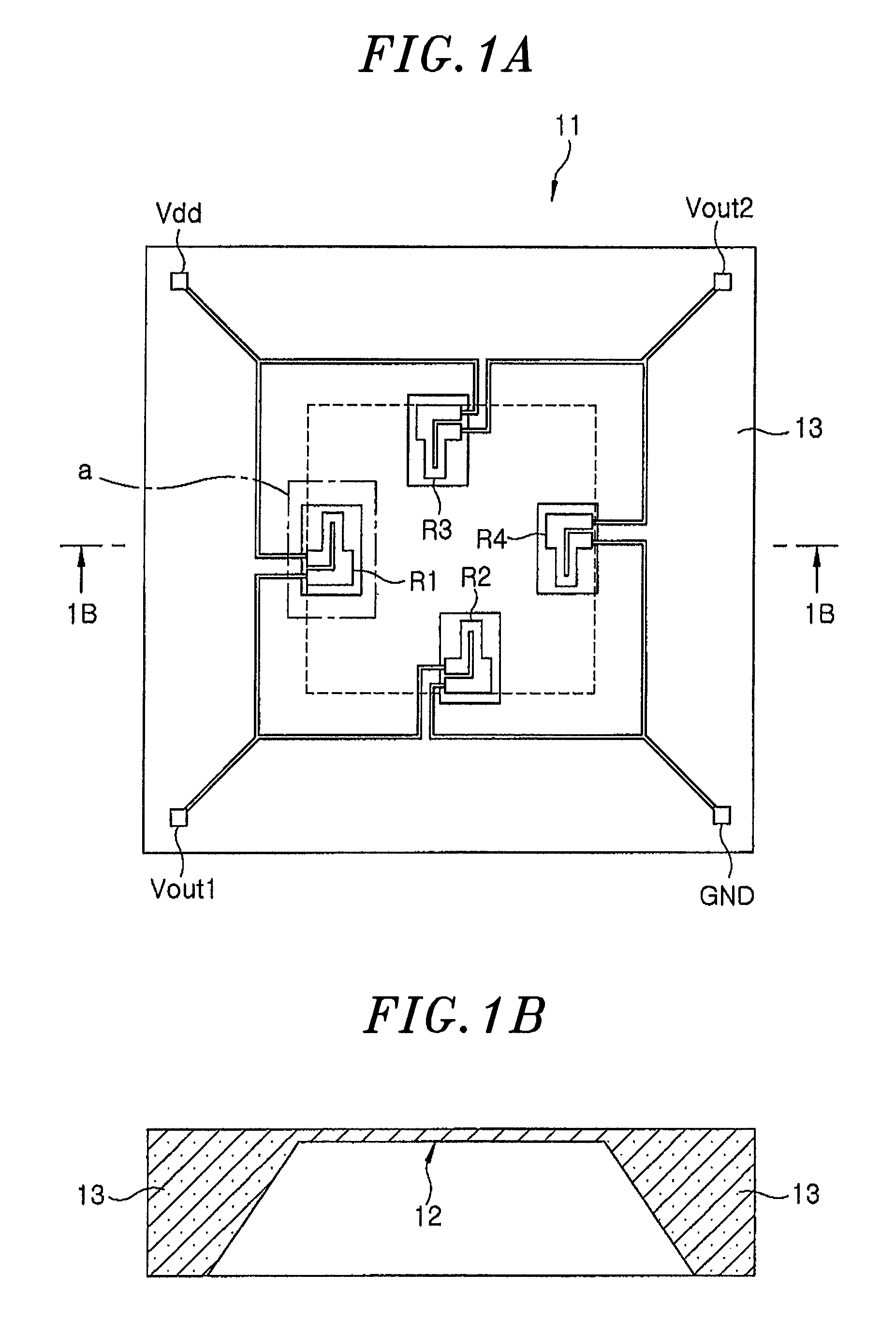
[0030]FIGS. 1A and 1B show a configuration of a semiconductor pressure sensor in accordance with a first embodiment of the present invention. FIG. 1A is a plan view of the semiconductor pressure sensor, and FIG. 1B is a cross-sectional view taken along line 1B-1B of FIG. 1A. As shown in FIGS. 1A and 1B, a semiconductor pressure sensor 11 in accordance with the first embodiment of the present invention includes a semiconductor substrate 13 which is made of, e.g., a single crystal silicon substrate and has a thin diaphragm 12 formed in a rectangular shape, and piezoresistive elements R1 to R4 which are respectively formed on a surface region of the semiconductor substrate 13 inside of four side of the diaphragm 12.

[0031]One end of the piezoresistive element R1 is connected to one end of the piezoresistive element R2 through, e.g., a diffusion wiring, and the connection node is connected to an output terminal Vout1 of a Wheatstone bridge circuit to be described below. The other end of ...

second embodiment

[0042]FIG. 4 shows a configuration of a semiconductor pressure sensor in accordance with a second embodiment of the present invention. FIG. 4 corresponds to FIG. 3 of the first embodiment. Since the configuration and arrangement of each of the piezoresistive elements R1 to R4 are the same as those in FIGS. 1A to 2B of the first embodiment, a description thereof will be omitted.

[0043]In contrast to the first embodiment, the second embodiment is characterized in that the n-type semiconductor regions 21 respectively including the piezoresistive elements R1 to R4 are connected commonly to a wiring 41 made of a diffusion layer, a metal or the like, and connected to the high voltage Vdd of the Wheatstone bridge circuit.

[0044]With such configuration, in the second embodiment, it is possible to apply a potential of the high voltage to the shielding thin film layers 23 through the respective n-type semiconductor regions 21. Thus, the potentials of the shielding thin film layers 23 can be sim...

third embodiment

[0045]FIG. 5 shows a configuration of a semiconductor pressure sensor in accordance with a third embodiment of the present invention. FIG. 5 corresponds to FIG. 3 of the first embodiment. Since the configuration and arrangement of each of the piezoresistive elements R1 to R4 are the same as those in FIGS. 1A to 2B of the first embodiment, a description thereof will be omitted.

[0046]In contrast to the first embodiment, the third embodiment is characterized in that the n-type semiconductor regions 21 respectively including the piezoresistive elements R1 and R3, one end of each of which is connected to the high voltage Vdd, are connected to each other through a wiring 51 made of a diffusion layer, a metal or the like. The third embodiment is further characterized in that the n-type semiconductor regions 21 respectively including the piezoresistive elements R2 and R4, one end of each of which is connected to the ground GND, are connected to each other through a wiring 52 made of a diffu...


PUM

PropertyMeasurementUnit
n-type semiconductoraaaaaaaaaa
conductiveaaaaaaaaaa
voltageaaaaaaaaaa

Abstract

A semiconductor pressure sensor includes n-type semiconductor regions, which are formed in a diaphragm of a semiconductor substrate, piezoresistive elements, which are respectively formed in the n-type semiconductor regions, and conductive shielding thin film layers, which are respectively formed on the piezoresistive elements through an insulating thin film layer, and the piezoresistive elements form a Wheatstone bridge circuit. Further, the n-type semiconductor regions and the conductive shielding thin film layers are electrically connected to each other through contacts formed in the diaphragm.

Description

FIELD OF THE INVENTION[0001]The present invention relates to a semiconductor pressure sensor for use in detecting a pressure applied to a diaphragm by using a Wheatstone bridge circuit constituted by piezoresistive elements formed on the diaphragm.BACKGROUND OF THE INVENTION[0002]Conventionally, there has been developed a semiconductor pressure sensor in which piezoresistive elements (strain gauge resistive elements) are respectively disposed at separate locations on a surface of a diaphragm to form a Wheatstone bridge circuit. The semiconductor pressure sensor detects deflection occurring in the diaphragm when a pressure is applied to the sensor by detecting a change in the output voltage of the Wheatstone bridge circuit due to the applied bias according to a change in the resistance of the piezoresistive elements.[0003]In such a semiconductor pressure sensor, an offset voltage (output voltage of the Wheatstone bridge circuit when no pressure is applied to the sensor) varies when t...

Claims


Application Information

Patent Timeline
Patent Type & Authority Patents(United States)
IPC IPC(8): H01L41/113H01L29/84B81B3/00G01L9/00
CPCB81B3/0086H01L29/84G01L9/00G01L9/0054
Inventor NIIMURA, YUICHINISHIKAWA, HIDEOKATO, FUMIHITO
Owner PANASONIC CORP
Why Eureka
Eureka Blog
Learn More