Pixel circuit and display device
a display device and pixel technology, applied in the field of display devices, can solve the problems of creeping of pixel electrode potential, creeping of creeping, and perception of creeping flickering, so as to reduce the power consumption of display, reduce the effect of polarity inversion interval and increase the polarity inversion interval
- Summary
- Abstract
- Description
- Claims
- Application Information
AI Technical Summary
Benefits of technology
Problems solved by technology
Method used
Image

Examples
first embodiment
1. First Embodiment
[0176]
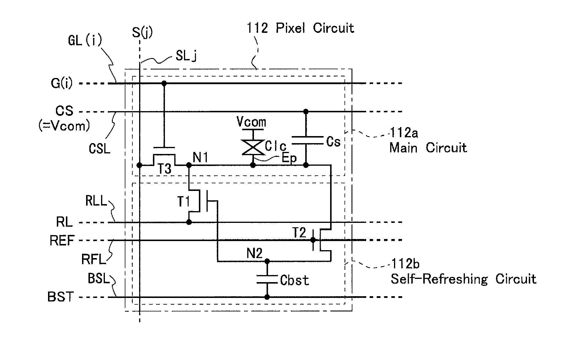
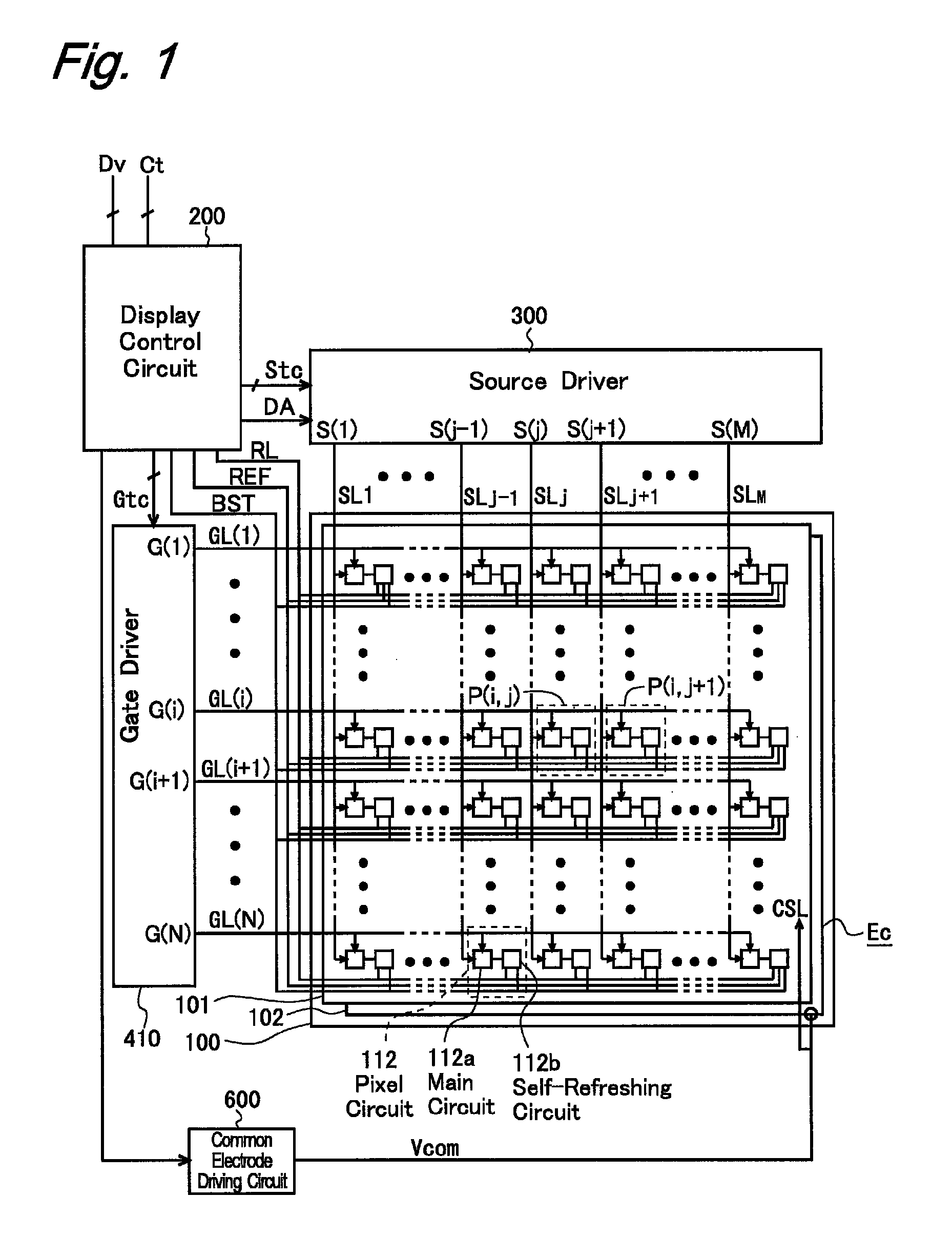
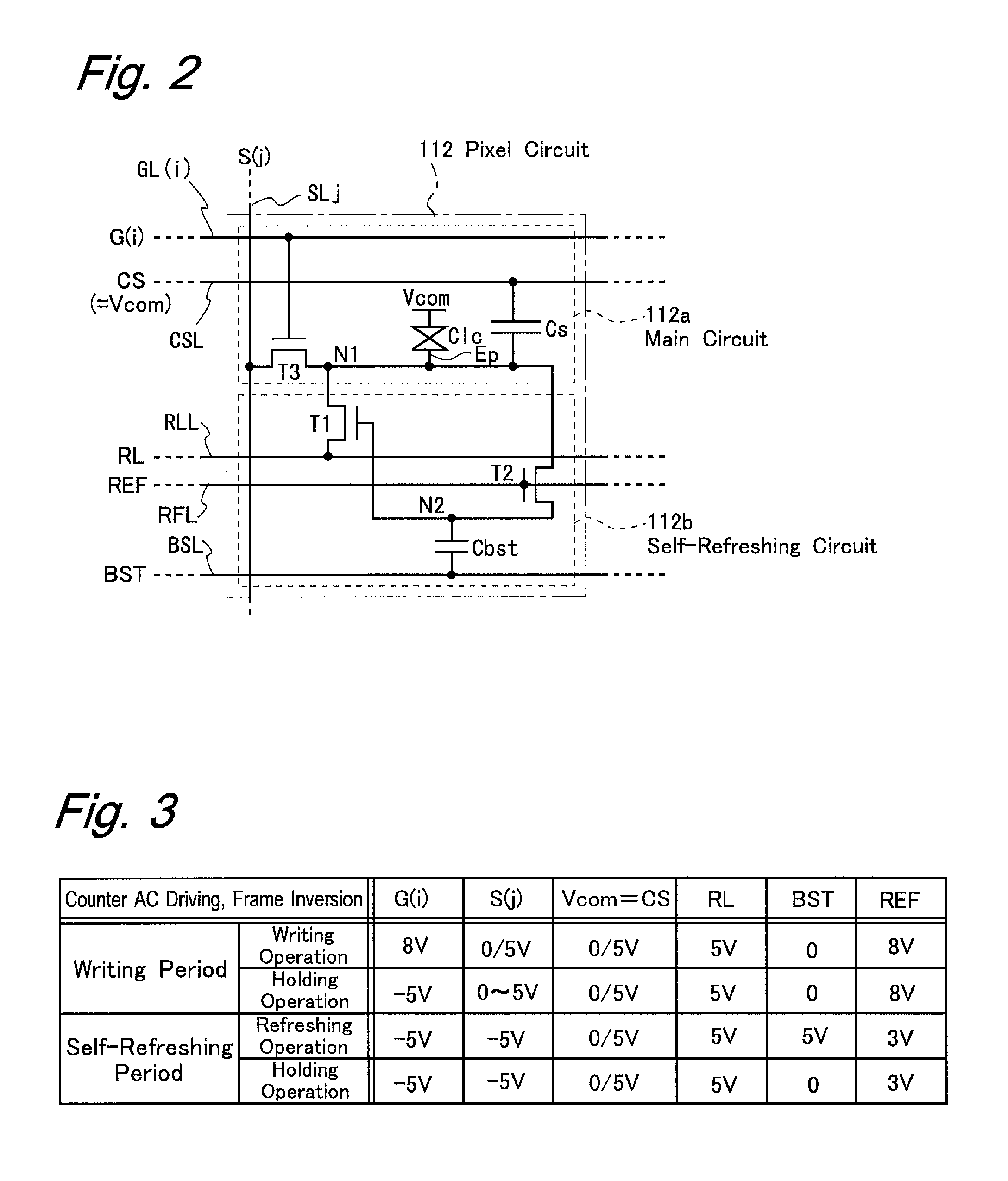
[0177]FIG. 1 is a block diagram showing a configuration of a liquid crystal display device according to a first embodiment of the present invention. FIG. 2 is a circuit diagram showing a configuration of a pixel circuit 112 according to the embodiment. The liquid crystal display device according to the present embodiment has a transparent, normal display mode, and a reflective, permanent display mode. The permanent display mode has a writing mode, a refreshing mode and a polarity inverting mode. The normal display mode is an operation mode employed in normal use, e.g., for movie display when this liquid crystal display device is incorporated in a mobile phone and is required to operate in a transparent mode, whereas the permanent display mode is an operation mode when still images are displayed in a reflective mode under low power consumption. Note, however, that the present invention is not limited to such an application and / or configuration as the above.
[0...
PUM
 Abstract
Description
Claims
Application Information
 - R&D
- Intellectual Property
- Life Sciences
- Materials
- Tech Scout
- Unparalleled Data Quality
- Higher Quality Content
- 60% Fewer Hallucinations
Browse by: Latest US Patents, China's latest patents, Technical Efficacy Thesaurus, Application Domain, Technology Topic, Popular Technical Reports.
© 2025 PatSnap. All rights reserved.Legal|Privacy policy|Modern Slavery Act Transparency Statement|Sitemap|About US| Contact US: help@patsnap.com