
Method for producing graphene oxide with tunable gap

a graphene oxide and gap technology, applied in the direction of solid-state devices, chemistry apparatus and processes, thermoelectric devices, etc., can solve the problems of limiting usability, significantly long time to complete, and less than ideal wet oxidation process, so as to achieve more expedient oxidation and safer oxidation treatment

Active Publication Date: 2013-12-17
CALIFORNIA INST OF TECH
View PDF7 Cites 1 Cited by
  • Summary
  • Abstract
  • Description
  • Claims
  • Application Information

AI Technical Summary

Benefits of technology

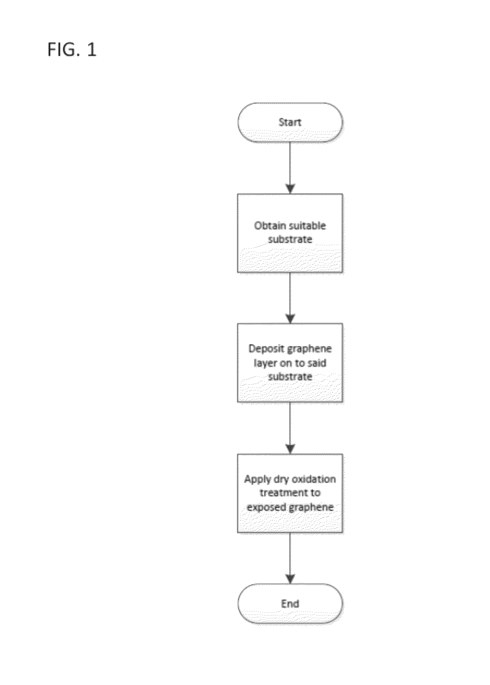
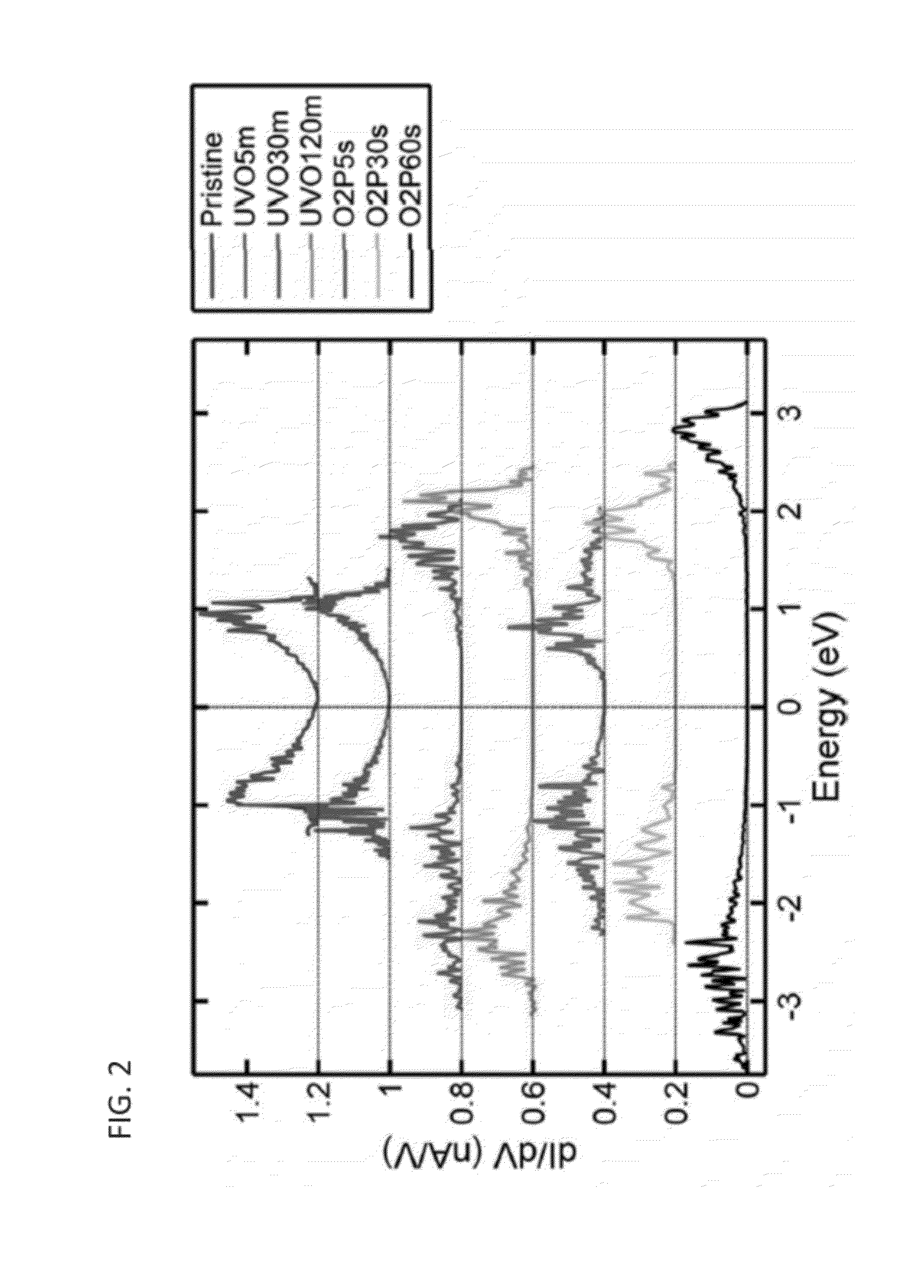
[0009]The present invention is directed to a novel fabrication method that allows for a versatile but precise manipulation of graphene so as to develop graphene oxide material that possesses an appreciable, and determinable, band gap, and in which the oxidation is confined to the graphene layer. This novel fabrication method can thus develop graphene oxides that are optimized for practical use. The process includes subjecting a graphene sample to a dry oxidation process for a pre-determined period of time, wherein the length of oxidation exposure determines the magnitude of the band gap.
[0012]In still another embodiment, a remote indirect plasma oxidation treatment, which allows for more expedient oxidation while providing a safer oxidation treatment as compared to a direct plasma oxidation treatment, is used as the oxidation process.

Problems solved by technology

However, graphene is inherently a semimetallic material—as opposed to a semiconductor material—and this limits its usability.
However, the wet oxidation process is less than ideal: it typically uses harsh chemicals, such as strong acids and oxidizing agents; it takes a significantly long time to complete; and it does not allow for the creation of site specific oxidation, which substantially limits the usability of this modified graphene.
At a higher defect density, a continuous decay and smoothing of the van Hove singularities becomes apparent, and a further increase in the defect density results in a significant drop in the conductance.
These studies also show that an increase in defect density becomes increasingly difficult as the oxygen adsorption reaches a constant value after a certain UV / ozone exposure time.
As the oxygen plasma exposure increases further, the level of disorder in the structural symmetry of graphene becomes more pronounced, which leads to a decrease in conductance and mobility, as well as a transition from semimetallic to semiconducting behavior.
However, the prior art has yet to develop a process for the production of a semiconductor graphene oxide material suitable for practical applications.
For example, although Nourbakhsh et al. discuss characterizing a graphene oxide layer created by a plasma oxidation process, the authors do not provide any guidance on how to avoid the creation of oxides on the substrate surface.

Method used


Image

  • Method for producing graphene oxide with tunable gap
  • Method for producing graphene oxide with tunable gap
  • Method for producing graphene oxide with tunable gap

Examples


example 1

Band Gap Studies

[0054]The atomically resolved image of pristine graphene samples obtained by scanning tunneling microscope (STM) exhibits a highly-symmetric hexagonal lattice structures, which is a typical signature of a pristine graphene layer. In agreement with previously reported study, these hexagonal lattice structures show an atomic spacing of ˜0.23 nm (FIG. 7b). (See, e.g., Mizes H A, et al., Physical Review B. 1987, 36, 4491, the disclosure of which is incorporated herein by reference.) Three distinct peaks of D band (˜1350 cm−1), G band (˜1580 cm−1) and G′ band (˜2700) can be seen in the Raman spectrum of the pristine graphene samples (FIG. 7c). (See, e.g., Dresselhaus M S, et al., Nano Lett. 2010, 10, 751-8; Reina A, et al., Nano Lett 2009, 9, 30-5; and Dresselhaus M S, et al., Annual Review of Condensed Matter Physics. 2010, 1, 89-108, the disclosure of which is incorporated herein by reference.) The peak intensity ratio between the disorder-induced D band and sp2 symmetr...

example 2

XPS Studies

[0063]The presence of oxygen adsorbates in the oxidized graphene samples was further investigated using high-resolution XPS scans. Curve-fitting and deconvolution of the high-resolution XPS spectra of C 1s was performed using a Gaussian-Lorentzian peak shape with Shirley baseline correction. Deconvolution of the C 1s XPS spectra of both oxygen plasma and UV / ozone treated samples shows four distinct peaks associated with sp2 C—C (284.7±0.1 eV, FWHM 0.9 eV), C—O (285.2±0.1 eV, FWHM 1.45 eV), C═O (286.7±0.1 eV, FWHM 1.45 eV), and O—C═O (288.6±0.1 eV, FWHM 4 eV). (See, Yang D, et al., Carbon. 2009, 47, 145-52, the disclosure of which is incorporated herein by reference.) The C 1s XPS spectra of the pristine graphene samples show a very strong C—O peak which may be caused by a significant presence of hydroxyl or epoxide groups at the edge. These spectra also show a relatively weak C═O peak and the absence of a peak associated with O—C═O group (FIG. 9a). The O—C═O peak can be b...

example 3

STM Studies

[0068]The effect of both oxygen plasma and UV / ozone treatments to the electronic structure of graphene can be literally seen from the evolution of the atomically resolved images obtained by scanning tunneling microscope (STM). As graphene is oxidized, defects on the hexagonal lattice structure due to the presence of oxygen adsorbates in the form of oxygenated functional groups start to occur. For samples with low concentration of oxygen adsorbates, i.e. O2P5s and UVO5m samples, the degree of disorder is quite low such that the hexagonal lattice structures still can be recognized from the raw STM images without using any further image processing technique (FIG. 12a). At higher concentration of oxygen adsorbates, the distortion to the lattice structure is amplified such that the hexagonal patterns become much less apparent and more difficult to be recognized from the raw STM images. Fourier transformation of the raw STM images of O2P10s and UVO30m samples reveals a superpos...


PUM

PropertyMeasurementUnit
band gapaaaaaaaaaa
band gapaaaaaaaaaa
energy gapaaaaaaaaaa

Abstract

A method of fabricating a graphene oxide material in which oxidation is confined within the graphene layer and that possesses a desired band gap is provided. The method allows specific band gap values to be developed. Additionally, the use of masks is consistent with the method, so intricate configurations can be achieved. The resulting graphene oxide material is thus completely customizable and can be adapted to a plethora of useful engineering applications.

Description

RELATED APPLICATIONS[0001]The current application claims priority to U.S. Provisional Application No. 61 / 422,092, filed Dec. 10, 2010, the disclosure of which is incorporated herein by reference.FIELD OF THE INVENTION[0002]The current invention is directed toward a method for producing a semiconducting graphene oxide material in which the oxidation is confined to the graphene layer.BACKGROUND OF THE INVENTION[0003]Graphene, a material comprising a lattice of carbon atoms positioned in a ‘honeycomb-type’ arrangement and tightly joined by in-plane sp2 bonds, has garnered much attention from research communities because its unique electrical and mechanical properties make it potentially ideally suited for various engineering applications, such as nanoelectronics and integrated circuits. Compared to other conductive and semiconductive materials, graphene has a superior carrier mobility and low resistivity, making it a promising candidate for integrated circuits. (Castro Neto A H, et al....

Claims


Application Information

Patent Timeline
Patent Type & Authority Patents(United States)
IPC IPC(8): H01L51/40H01L29/08
CPCC01B31/043C01B31/0484H01L21/02527H01L21/02614B82Y30/00B82Y40/00C01B32/23C01B32/186C01B32/194Y10S977/734Y10S977/843Y10S977/847Y10S977/932H01L29/24
Inventor GHARIB, MORTEZAARIA, ADRIANUS INDRATGANI, ADI WIJAYA
Owner CALIFORNIA INST OF TECH
Learn More