
System for inspecting defects of panel device

a panel device and defect technology, applied in the field of system for inspecting defects of panel devices, can solve the problems of various defects that are inspected, defects on the surface or in the inner parts of the display panel or the transparent element, foreign particles adhering to the surface, etc., to improve the performance of inspection of defects

Inactive Publication Date: 2013-10-29
IND TECH RES INST
View PDF22 Cites 1 Cited by
  • Summary
  • Abstract
  • Description
  • Claims
  • Application Information

AI Technical Summary

Benefits of technology

[0009]Accordingly, the present invention is directed to a system for inspecting defects of a panel device, which uses improved light source apparatus to at least improve the performance of inspecting defects of the device.

Problems solved by technology

For example, during the manufacturing process, the elements of the display panel or the transparent elements may have defects on their surfaces or in their inner parts.
The defects include various defects that are inspected by light beam, for example, foreign particles adhered on the surfaces, surface cracks, and the like or foreign particles, holes, or cracks of the inner parts, and the like.
The light box manufactured by the fluorescent lamps has disadvantages of bulk volume and large thickness, and needs a semi-transparent diffuser and a reflective manner to uniform the light beam.
However, the diffuser may attenuate the intensity of the light, so the brightness of the fluorescent lamp must be increased for compensation, which is power consuming and increases the manufacturing cost.
In addition, since the physical characteristics of the fluorescent lamps can only achieve a multi-level dimming, the generated light color is limited to the white light and the day light, and thus the adjustment scope is limited.

Method used

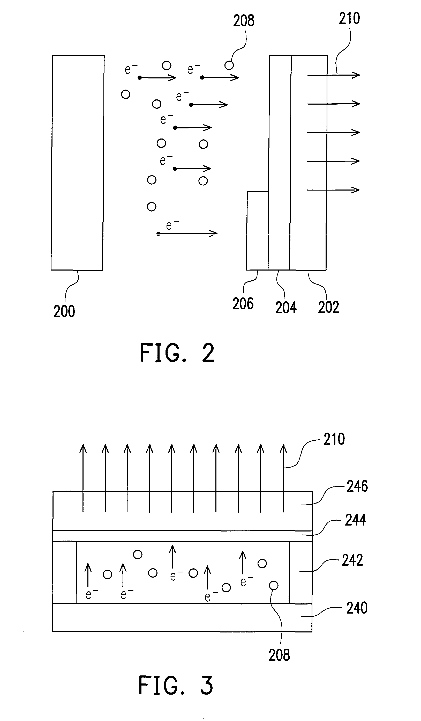

Image

  • System for inspecting defects of panel device
  • System for inspecting defects of panel device
  • System for inspecting defects of panel device

Examples


Embodiment Construction

[0023]Reference will now be made in detail to the present embodiments of the invention, examples of which are illustrated in the accompanying drawings. Wherever possible, the same reference numbers are used in the drawings and the description to refer to the same or like parts.

[0024]The present invention is, for example, applicable to a flat light source equipment for product inspection in the production lines. The present invention provides a flat electron emission lamp (FEEL) serving as the inspection light source, which can be used as the light source of the inspection light box. Here, the flat light source refers to the surface light source, and the surface may be curving surface or planar surface as required.

[0025]The light source of the inspection light box is the FEEL instead since the FEEL is a flat light source and does not need the diffuser, thereby reducing the light loss. In addition, the light source apparatus of the present invention may be fabricated into light source...


PUM

PropertyMeasurementUnit
fluorescentaaaaaaaaaa
pressureaaaaaaaaaa
surface structureaaaaaaaaaa

Abstract

System for inspecting defects of panel device includes a to-be-inspected device, a platform for holding the to-be-inspected device, a power unit, and a light source apparatus. The light source apparatus is controlled by the power unit to provide an inspection light to the to-be-inspected device for inspecting whether or not having defects. The light source apparatus includes a cathode structure, an anode structure, a fluorescent layer, and a low-pressure gas layer. The fluorescent layer is located between the cathode structure and the anode structure. The low-pressure gas layer is filled between the cathode structure and the anode structure, for inducing the cathode to emit electrons uniformly. The low-pressure gas layer has an electron mean free path, allowing at least enough electrons to directly hit the fluorescent layer under an operating voltage.

Description

CROSS-REFERENCE TO RELATED APPLICATION[0001]This application claims the priority benefit of Taiwan application serial no. 97111527, filed on Mar. 28, 2008. The entirety of the above-mentioned patent application is hereby incorporated by reference herein and made a part of this specification.BACKGROUND OF THE INVENTION[0002]1. Field of the Invention[0003]The present invention generally relates to a system for inspecting defects of a panel device, capable of, for example, inspecting the optically detected defects on a panel device.[0004]2. Description of Related Art[0005]Defect inspection of devices is a necessary process for reducing performance defects of final products. For example, during the manufacturing process, the elements of the display panel or the transparent elements may have defects on their surfaces or in their inner parts. The defects include various defects that are inspected by light beam, for example, foreign particles adhered on the surfaces, surface cracks, and th...

Claims


Application Information

Patent Timeline
Patent Type & Authority Patents(United States)
IPC IPC(8): G01N21/00
CPCG01N21/8803
Inventor LI, JUNG-YUCHEN, SHIH-PULIN, YI-PINGCHO, LIAN-YI
Owner IND TECH RES INST
Learn More