Top-emitting nitride-based light-emitting device with ohmic characteristics and luminous efficiency
a technology of ohmic characteristics and luminous efficiency, which is applied in the direction of solid-state devices, electric lighting sources, electric light sources, etc., can solve the problems of high light reflectivity, low work function, and inability to meet the requirements of large-area, high-brightness, and large-capacity light-emitting devices. , to achieve the effect of low specific ohmic contact resistance, low light transmittance, and low work function
- Summary
- Abstract
- Description
- Claims
- Application Information
AI Technical Summary
Benefits of technology
Problems solved by technology
Method used
Image
Examples
first embodiment
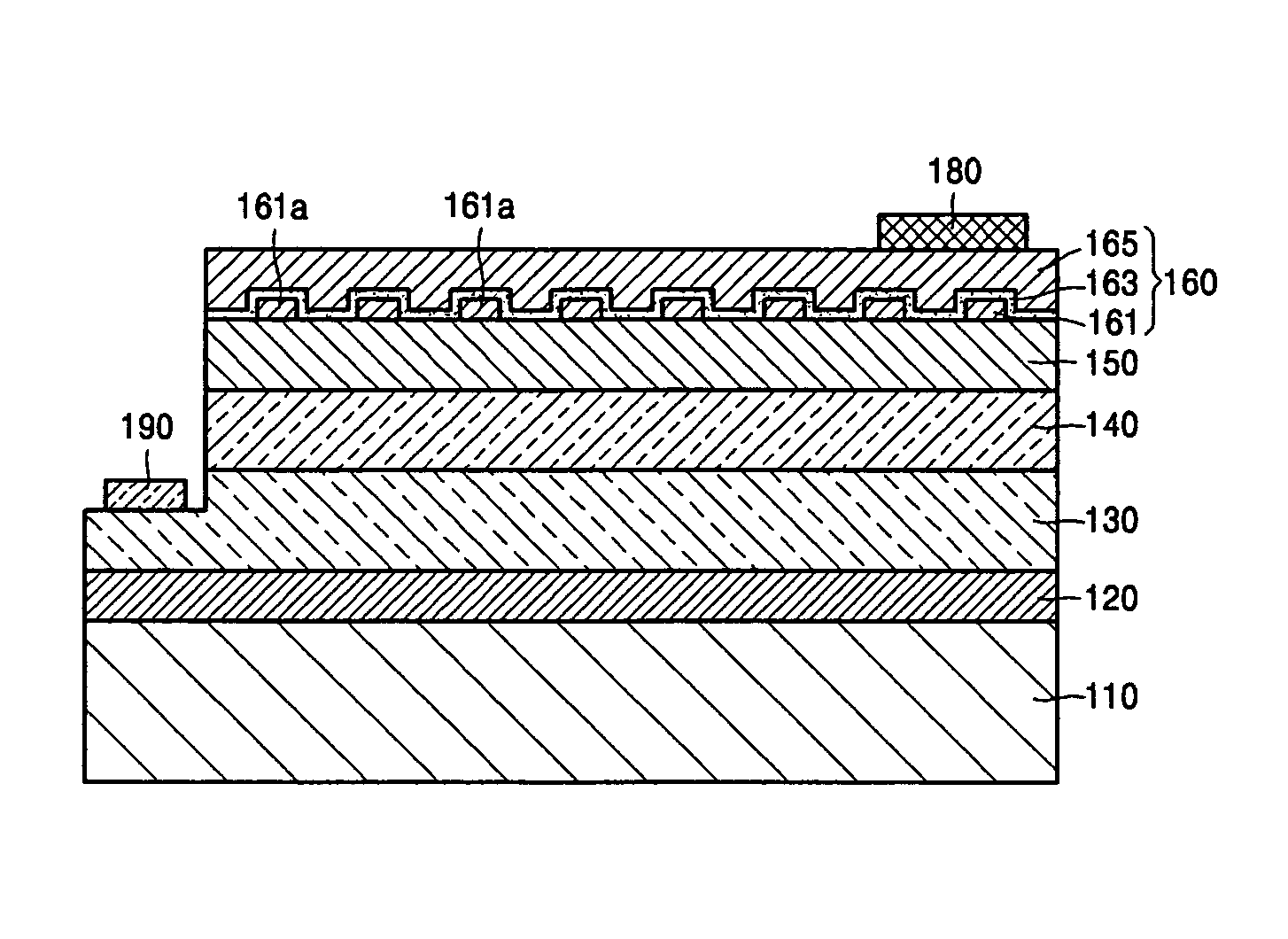
[0038]Referring to FIG. 1, a top-emitting light-emitting device according to the present invention includes a substrate 110, and a buffer layer 120, an n-cladding layer 130, an active layer 140, a p-cladding layer 150 and a transparent multilayer ohmic contact 160 sequentially formed on the substrate 110. The top-emitting light-emitting device further includes a p-electrode pad 180 and an n-electrode pad 190.
[0039]The top-emitting light-emitting device is mainly divided into a light-emitting structure including the substrate 110, the buffer layer 120, the n-cladding layer 130, the active layer 140, and the p-cladding layer 150 and a p-electrode structure including the transparent multilayer ohmic contact 160 formed on the p-cladding layer 150. The substrate 110 may be formed from sapphire, silicon carbide (SiC), Si, or gallium arsenide (GaAs). Optionally, the buffer layer 120 may not be formed.
[0040]Each of the layers from the buffer layer 120 up to the p-cladding layer 150 includes...
second embodiment
[0055]A curve with dash marks on the graph represents light transmittance obtained by annealing a light-emitting device with a p-electrode structure according to the present invention at 530° C. The p-electrode structure comprises the grid cell layer 161 composed of a regular grid array of Au particles with a size of 20 μm on the p-cladding layer 150, the surface protective layer 163 formed by sequentially depositing Ni (5 nm) and Au (5 nm), and the transparent conducting layer 165 made of ITO with a thickness of 100 nm.
[0056]A curve with dot marks represents light transmittance obtained by annealing a light-emitting device with a conventional p-electrode structure formed by sequentially depositing Au (5 nm) and Ni (5 nm) on the p-cladding layer 150 at 530° C.
[0057]As evident from FIG. 3, the light-emitting devices according to the present invention exhibit improved light transmittances over the conventional light-emitting device. Furthermore, the light-emitting devices according to...
PUM
 Abstract
Description
Claims
Application Information
 - R&D
- Intellectual Property
- Life Sciences
- Materials
- Tech Scout
- Unparalleled Data Quality
- Higher Quality Content
- 60% Fewer Hallucinations
Browse by: Latest US Patents, China's latest patents, Technical Efficacy Thesaurus, Application Domain, Technology Topic, Popular Technical Reports.
© 2025 PatSnap. All rights reserved.Legal|Privacy policy|Modern Slavery Act Transparency Statement|Sitemap|About US| Contact US: help@patsnap.com


