
Display device

a display device and display screen technology, applied in the field of display devices, can solve the problems of large display device thickness, limited shape of non-planar screen, and easy vibration of optical systems, and achieve the effect of free from image distortion

Inactive Publication Date: 2013-02-12
MITSUBISHI ELECTRIC CORP
View PDF11 Cites 5 Cited by
  • Summary
  • Abstract
  • Description
  • Claims
  • Application Information

AI Technical Summary

Benefits of technology

[0018]The invention has been accomplished in order to solve the foregoing problems. An object of the invention is to provide a display device capable of configuring a nonplanar display face in a simple way on the side of an observer by using a planar display element and including a nonplanar display face capable of reducing distortions in an image when the observer watches the nonplanar display face from a predetermined direction.
[0020]According to the invention, it is possible to provide a display device including a nonplanar display face which readily presents a nonplanar display face to the observer through combination of a planar display element and an optical element and which are almost free from distortions in an image when the observer watches the nonplanar display face from a predetermined direction.

Problems solved by technology

The projector system has problems such as a large depth (thickness) of the display device and the optical system vulnerable to vibrations.
Thus, the shape of the nonplanar screen is limited.
This arrangement is simple but the material, thickness and heat resistance of the flexible substrate are limited.
It is currently difficult to manufacture a liquid crystal display panel of the active matrix type made of a thin-film transistor or the like that offers high picture quality.
The nonplanar display face has the shape of a simple curved face and the shapes of a nonplanar display face that may be manufactured are limited.
Depending on the shape of a particular nonplanar display face, uncorrectable distortions in an image are conspicuous.

Method used


Image

  • Display device
  • Display device
  • Display device

Examples


embodiment 1

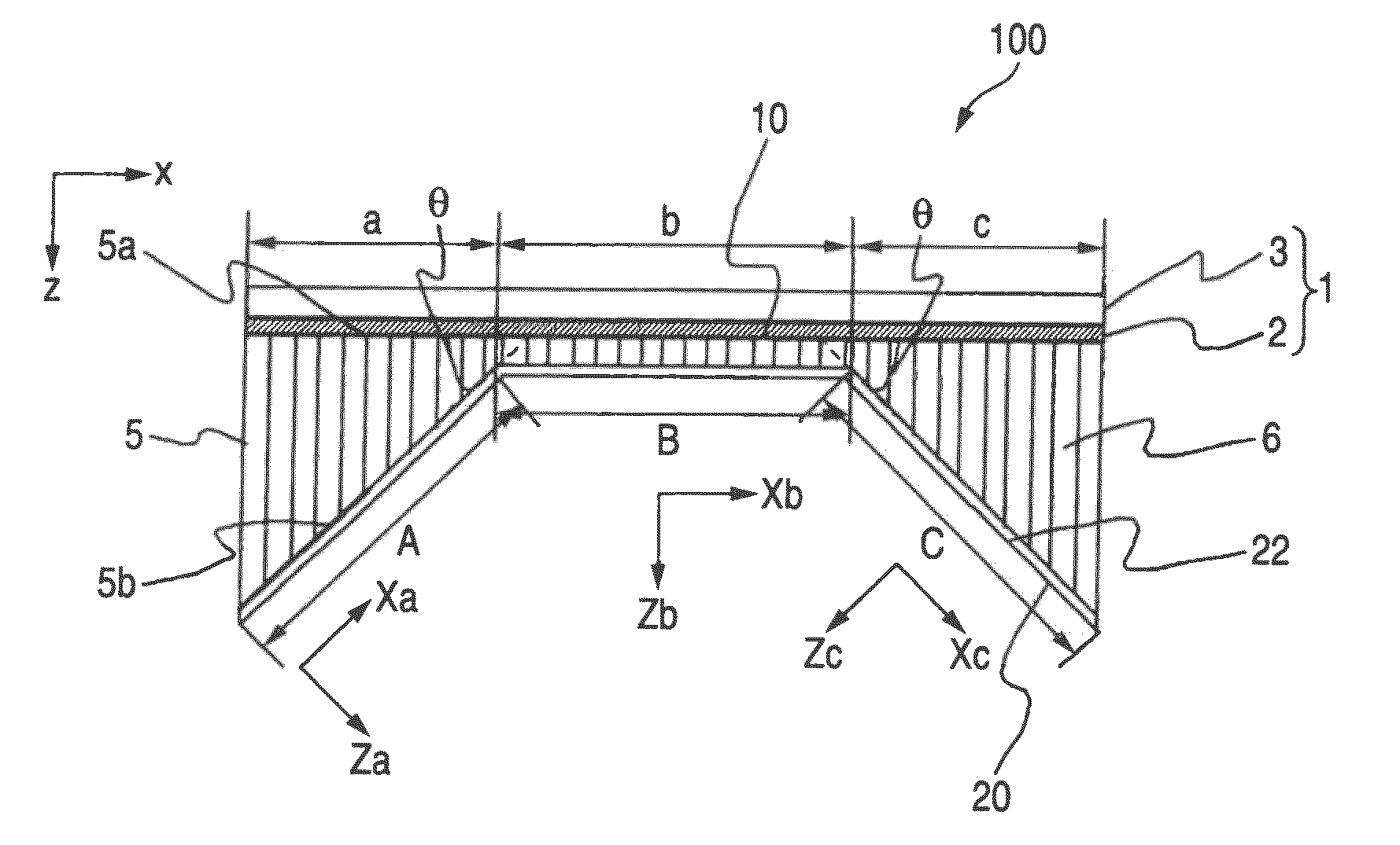
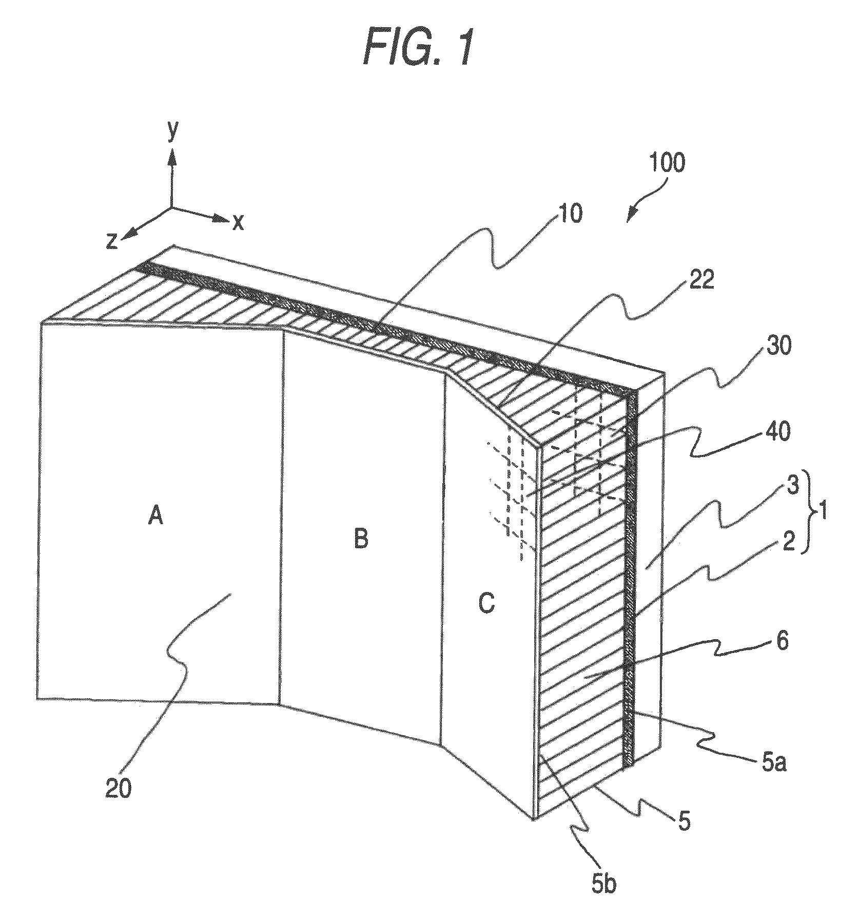
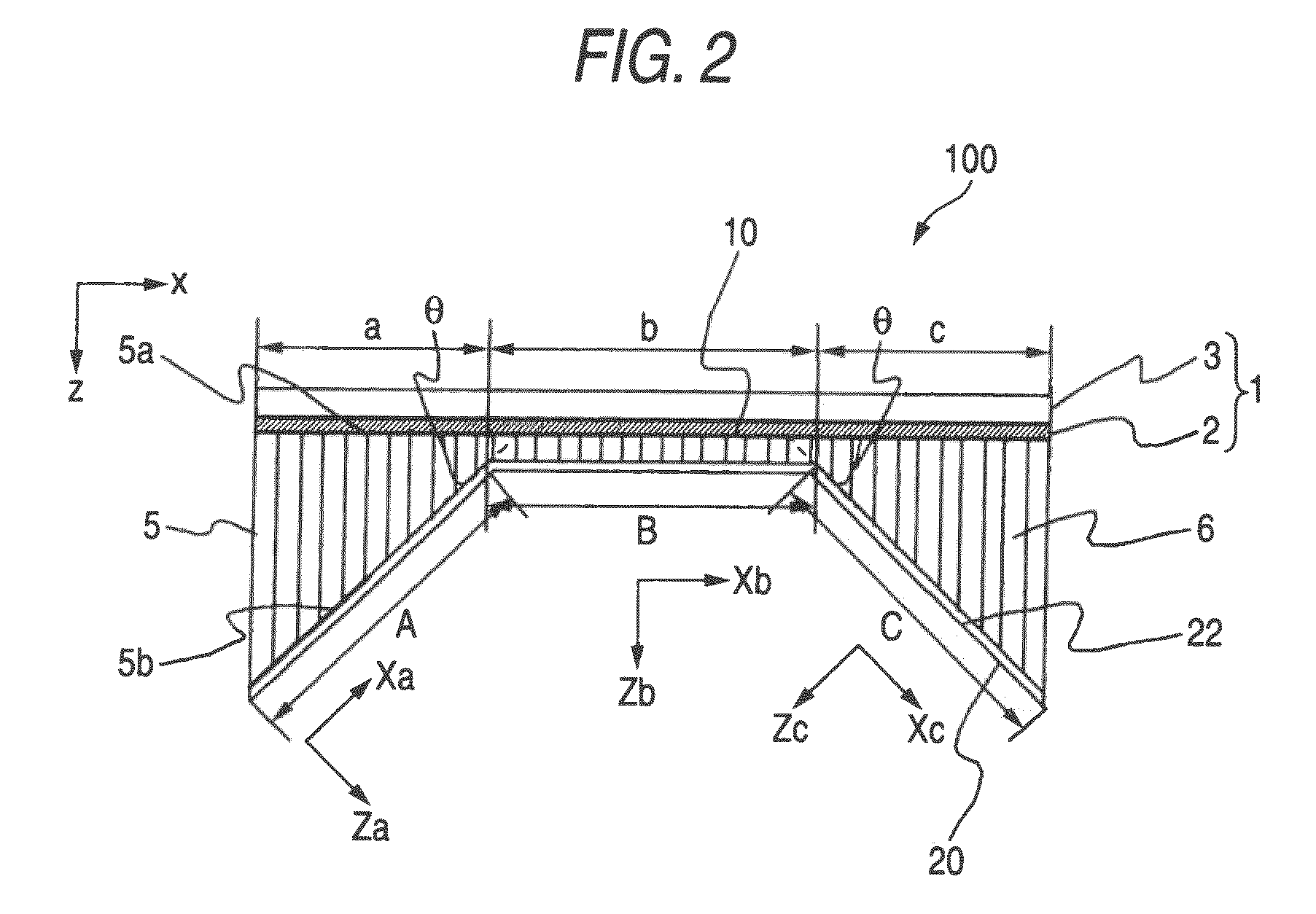
[0045]FIG. 1 is a perspective view of the general configuration of a display device according to Embodiment 1 of the invention. FIG. 2 is a top view of the display device shown in FIG. 1. FIG. 3 is a front view showing a plurality of pixels arranged in a matrix shape constituting the planar display face of a display element in the display device of FIG. 1. FIG. 4 is a front view showing the plurality of pixels arranged in a matrix shape with the nonplanar display face of the display device of FIG. 1 developed in horizontal direction.

[0046]In FIGS. 1 and 2, a display device 100 comprises a display element 1 including a liquid crystal display panel 2 having a planar display face 10 and a backlight 3, and an optical element 5 arranged in close contact with or in close proximity to the front surface of the entire planar display face 10. The optical element 5 is an assembly of a large number of optical paths having dimensions smaller than those of a pixel 30 of the planar display face 10...

embodiment 2

[0084]FIG. 8 is a perspective view of the general configuration of a display device according to Embodiment 2 of the invention. FIG. 9 is a top view of the display device shown in FIG. 8. FIG. 10 is a front view showing a plurality of pixels arranged in a matrix shape constituting the planar display face of a display element in the display device of FIG. 8. FIG. 11 is a front view showing the plurality of pixels arranged in a matrix shape with the nonplanar display face of the display device of FIG. 8 developed in horizontal direction.

[0085]While the optical element 5 is arranged on the entire planar display face 10 of the display element 1 in Embodiment 1, the optical element 5 formed of an optical fiber plate is arranged in a partial region of the planar display face 10 as shown in FIG. 8 in Embodiment 2.

[0086]As shown in FIG. 9, the optical element 5 is arranged in a right-hand region e of the planar display face 10, not in a left-hand region d of the planar display face 10. The ...

embodiment 3

[0095]FIG. 12 is a perspective view of the general configuration of a display device according to Embodiment 3 of the invention. FIG. 13 is a top view of the display device shown in FIG. 12. FIG. 14 is a front view showing a plurality of pixels arranged in a matrix shape constituting the planar display face of a display element in the display device of FIG. 12. FIG. 15 is a front view showing the plurality of pixels arranged in a matrix shape with the nonplanar display face of the display device of FIG. 12 developed in horizontal direction.

[0096]In Embodiment 3, the shape of the nonplanar display face 20 is the same as that of Embodiment 2. Embodiment 3 differs from Embodiment 2 in that the optical fibers 6 of the optical element 5 are arranged in the direction of the normal Zg in the region G of the nonplanar display face 20 rather than in the direction of normal in the region g of the planar display face 10, as shown in FIG. 13.

[0097]Also in such a configuration of the optical ele...


PUM


Abstract

A display device including a display element having a planar display face on which a plurality of pixels are arranged in a matrix shape and an optical element arranged in close contact with or in close proximity to at least a partial region of the planar display face and optically transmitting image light incoming from the planar display face to a light-emitting face, characterized in that the light-emitting face of the optical element has a surface not parallel to at least the planar display face and forms a nonplanar display face and that the plurality of pixels on the planar display face do not have the same dimensions but different dimensions in accordance with the angle θ formed by the planar display face and the nonplanar display face corresponding to the pixels of the planar display face.

Description

[0001]This application claims priority from Japanese Patent Application No. 2007-257268 filed on Oct. 1, 2007 and Japanese Patent Application No. 2008-174347 filed on Jul. 3, 2008, the entire subject matter of which is incorporated herein by reference.BACKGROUND OF THE INVENTION[0002]1. Field of the Invention[0003]The present invention relates to a display device and in particular to a display device including a nonplanar display face on the side of an observer such as a recessed, protruding or curved face instead of a planar display face.[0004]2. Description of the Related Art[0005]In recent years, display devices have been used in a variety of devices as means for displaying information to an observer. Current representative display devices have employed, in their main sections, new display elements using a liquid crystal display, a plasma display, an Electroluminescence (EL) display, a Field Emission Display (FED) or the like instead of a cathode-ray tube as a mainstay in the rel...

Claims


Application Information

Patent Timeline
Patent Type & Authority Patents(United States)
IPC IPC(8): G09G3/36
CPCG02F1/133524
Inventor ODOI, YUZOTOMITA, YOICHI
Owner MITSUBISHI ELECTRIC CORP
Learn More