Three-dimensional SoC structure formed by stacking multiple chip modules

a technology of stacking multiple chip modules and socs, applied in the direction of solid-state devices, basic electric elements, electrical apparatus construction details, etc., can solve the problems of inability to outsource, cannot solve the problem and the remaining part of the development process, so as to achieve the effect of reducing the overall volume of the system-on-chip

Active Publication Date: 2012-09-25
NAT APPLIED RES LAB
View PDF46 Cites 10 Cited by
  • Summary
  • Abstract
  • Description
  • Claims
  • Application Information

AI Technical Summary

Benefits of technology

[0008]It is an object of the present invention to provide a three-dimensional SoC structure formed by stacking multiple chip modules, wherein each connector module electrically connects two vertical SoC modules to form the three-dimensional SoC structure, thus effectively decreasing the overall volume of the system-on-chip.
[0009]It is another object of the present invention to provide a three-dimensional SoC structure formed by stacking multiple chip modules, wherein each vertical SoC module is constructed by stacking at least two chip modules vertically, thus increasing the number of preset elements in a unit area.
[0010]It is still another object of the present invention to provide a three-dimensional SoC structure formed by stacking multiple chip modules, wherein both vertical SoC modules and chip modules can be fabricated and verified in advance to shorten the verification process of the system-on-chip.

Problems solved by technology

While system developers may incorporate the silicon intellectual property (SIP) of external design teams during the design stage, the remaining part of the development process, particularly fabrication and verification, cannot be outsourced.
Although such a development process provides system developers with a high degree of autonomy and allows them to optimize product design at the latter stages, the costs of man power and time are lofty.

Method used


Image

  • Three-dimensional SoC structure formed by stacking multiple chip modules
  • Three-dimensional SoC structure formed by stacking multiple chip modules
  • Three-dimensional SoC structure formed by stacking multiple chip modules

Examples


Embodiment Construction

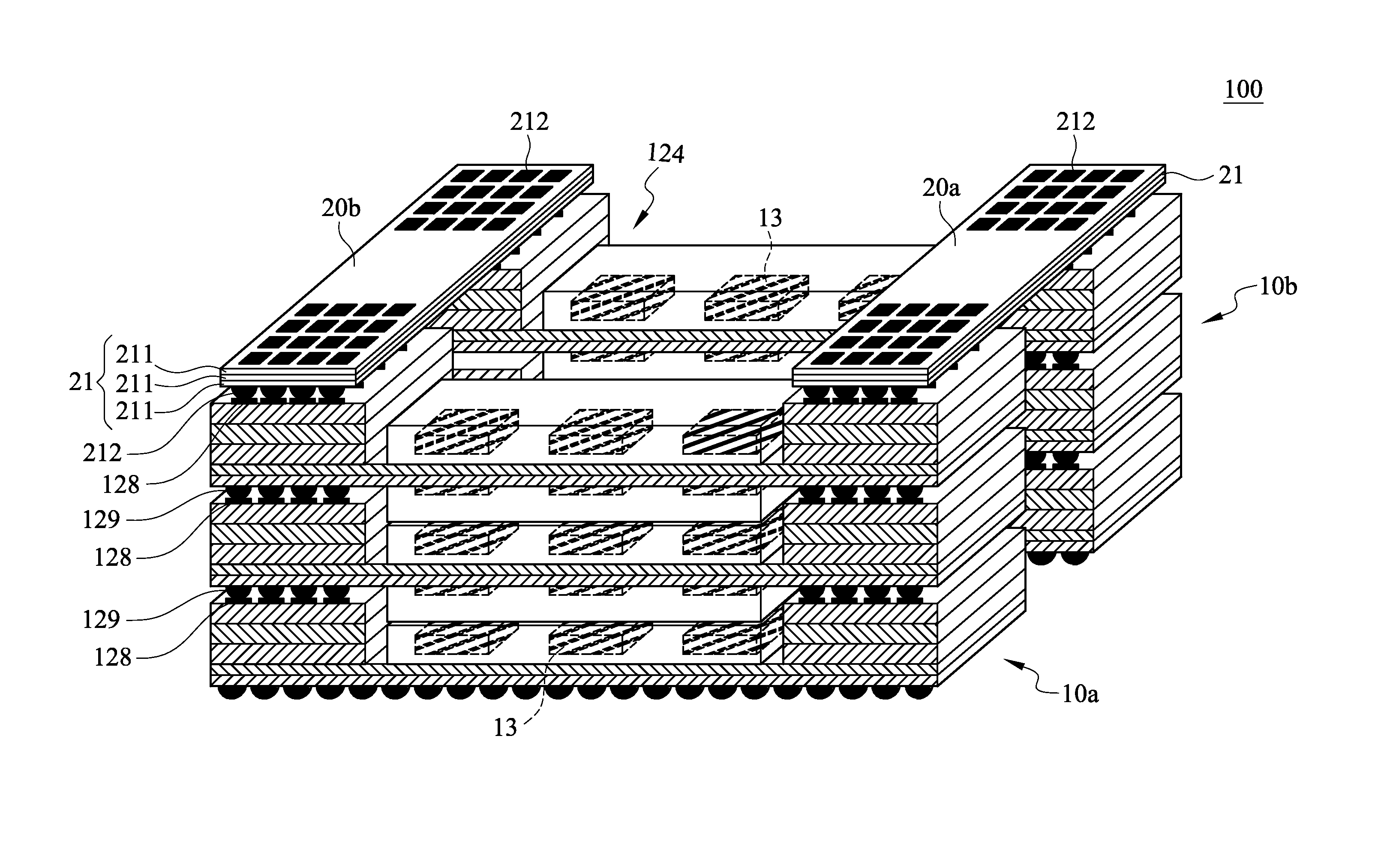
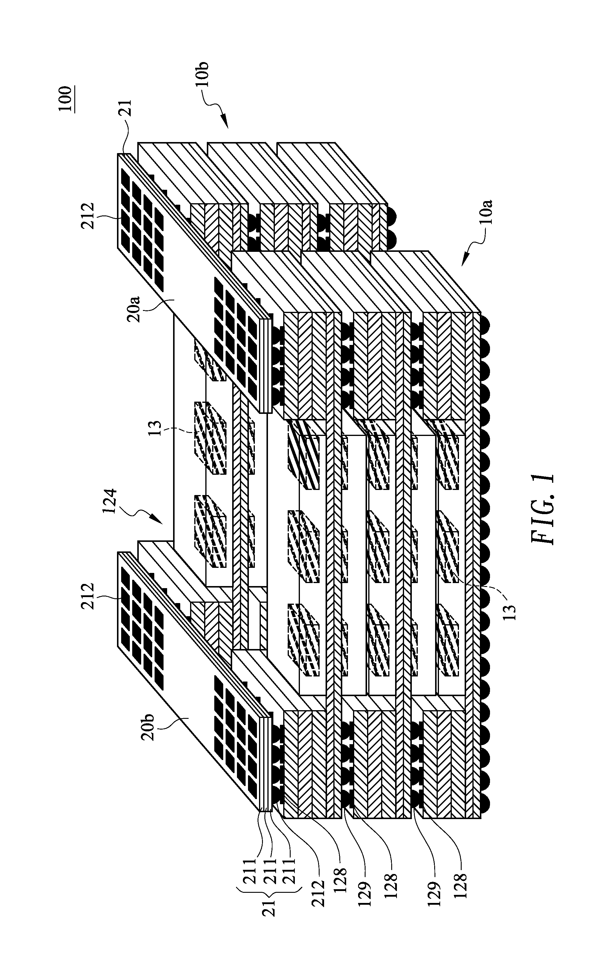
[0036]Referring to FIG. 1, a three-dimensional SoC structure 100 formed by stacking multiple chip modules according to an embodiment of the present invention includes at least two vertical SoC modules 10a, 10b and at least one connector module 20a, 20b.

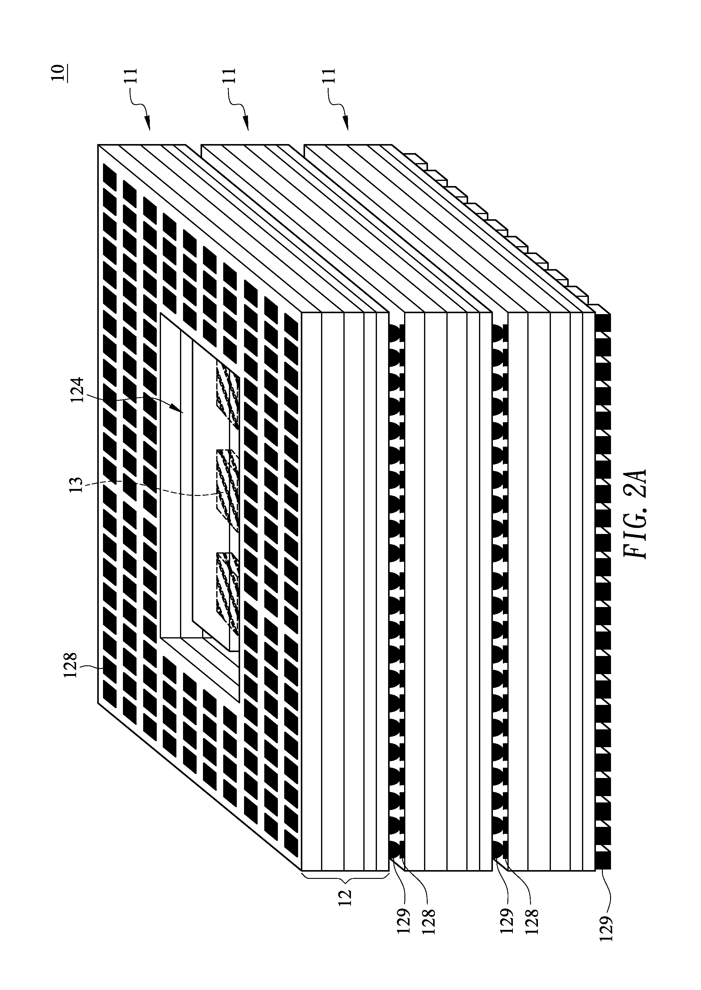
[0037]As shown in FIG. 2A through FIG. 2C, each vertical SoC module 10 is formed by stacking at least two chip modules 11 vertically. The chip modules 11 can be fabricated and packaged at the same time or sequentially. Thus, system designers only have to stack vertically and connect the packaged chip modules 11 to complete the fabrication of each vertical SoC module 10. Furthermore, as each chip module 11 is fabricated and verified in advance, the verification process of the system-on-chip can be shortened significantly, thereby reducing the time and costs of development.

[0038]Each chip module 11 includes a module circuit board 12 and at least one preset element 13.

[0039]With reference to FIG. 3A, the module circuit board 12 is compo...


PUM


Abstract

A three-dimensional SoC structure formed by stacking multiple chip modules is provided. The three-dimensional SoC structure includes at least two vertical SoC modules and at least one connector module, wherein each connector module electrically connects two vertical SoC modules. Each vertical SoC module is constructed by stacking at least two chip modules vertically. Each chip module includes a module circuit board and at least one preset element. A recess is formed in each module circuit board and provided with a first connecting interface for electrically connecting with the corresponding at least one preset element. The at least two vertical SoC modules are connected by the connector module to form a three-dimensional SoC structure with multiple functions. Besides, the recesses formed in the module circuit boards provide effective heat dissipation paths for the preset elements.

Description

BACKGROUND OF THE INVENTION[0001]1. Technical Field[0002]The present invention relates to a three-dimensional system-on-chip structure formed by stacking multiple chip modules. More particularly, the present invention relates to a three-dimensional system-on-chip structure which is formed by stacking a plurality of chip modules and applicable to system-on-chips.[0003]2. Description of Related Art[0004]A system-on-chip (SoC) refers to an integrated chip on a system level. In particular, a system-on-chip may include a computational element (e.g., a microprocessor, a digital signal processor, an image processor, etc.) as well as a memory, a logic circuit, an input / output circuit, and other connection circuits. In a nutshell, a system-on-chip is a single chip integrated with IC components which have different functions and are otherwise scattered in different chips. Therefore, a system-on-chip can be regarded as a single system having multiple functions.[0005]At the front-end design sta...

Claims


Application Information

Patent Timeline
Patent Type & Authority Patents(United States)
IPC IPC(8): H05K7/00H01L29/40H01L23/48H01L23/52
CPCH05K1/14H05K7/00H01L2924/15311H01L2224/16227H01L2924/15153H01L25/105H01L23/13H01L25/0657H01L25/0652H01L2924/00H01L2224/16225H01L25/18H01L2225/06517
Inventor HUANG, CHUN-MINGWEY, CHIN-LONGWU, CHIEN-MINGYANG, CHIH-CHYAUCHEN, SHIH-LUNCHEN, CHI-SHILIN, CHI-SHENG
Owner NAT APPLIED RES LAB
Why Eureka
Try Eureka