Plasma display and method for driving plasma display panel
a plasma display and plasma technology, applied in the direction of instruments, computing, electric digital data processing, etc., can solve the problems of increasing the load and temperature increasing the power consumption and costs of the driving circuit, and destroying the protective layer, etc., to solve or reduce one or more problems.
- Summary
- Abstract
- Description
- Claims
- Application Information
AI Technical Summary
Benefits of technology
Problems solved by technology
Method used
Image
Examples
first embodiment
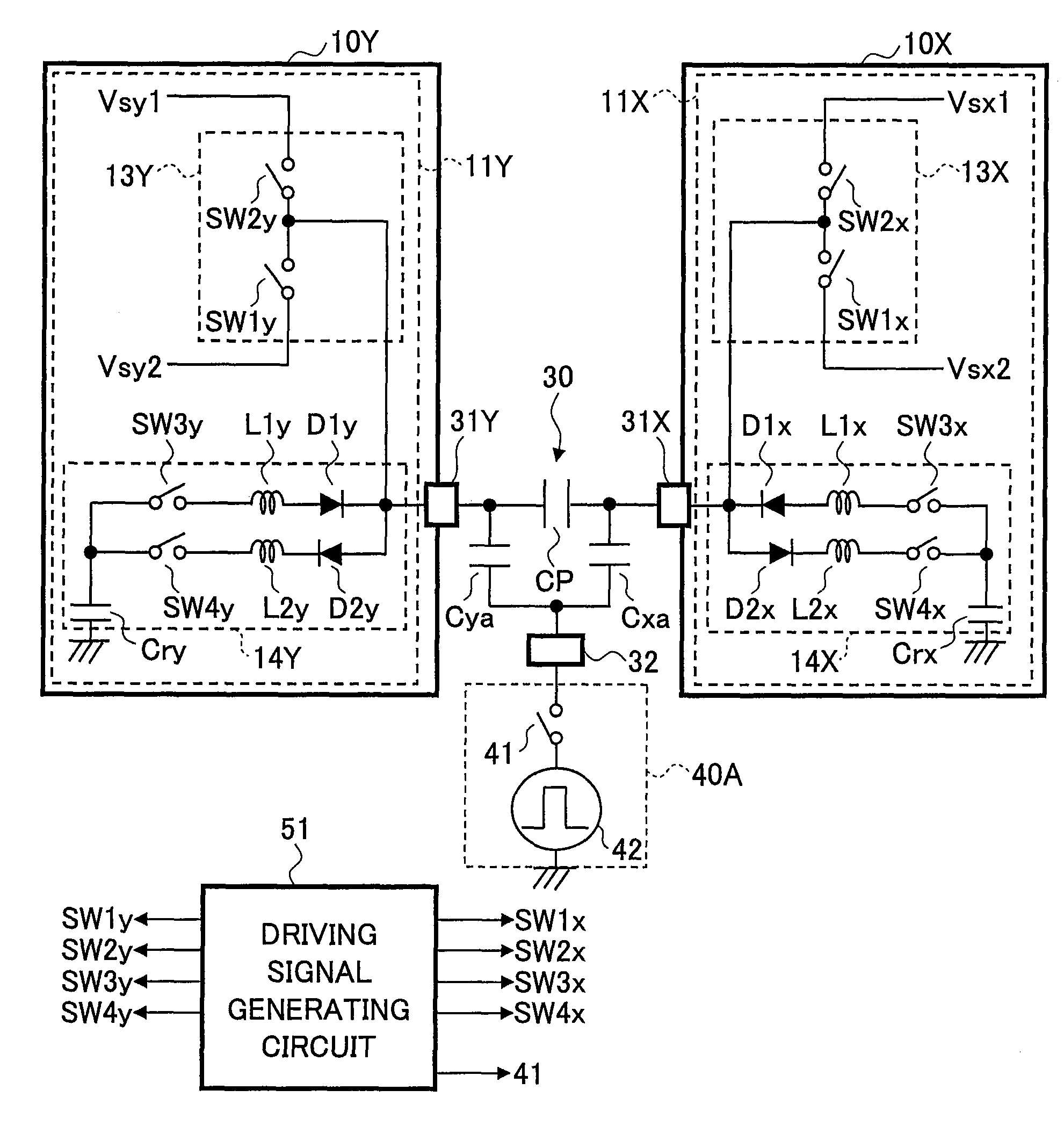
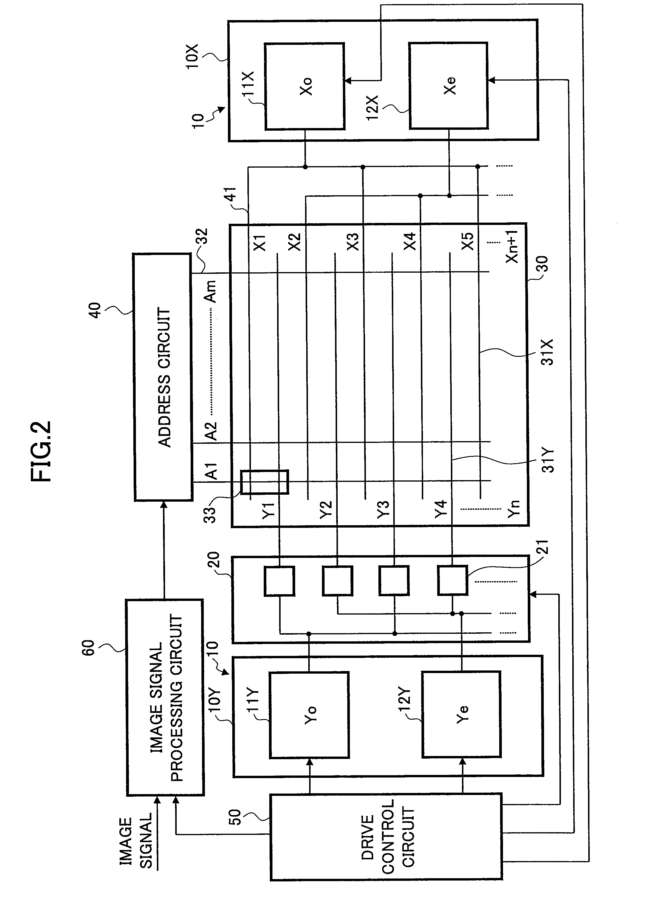
[0032]FIG. 2 is a schematic diagram illustrating a configuration of a plasma display according to a first embodiment of the present invention. A plasma display of this embodiment includes electrode driving circuits 10 including a Y-electrode driving circuit 10Y and an X-electrode driving circuit 10X, a scanning circuit 20, a plasma display panel (PDP) 30, an address circuit 40, a drive control circuit 50, and an image signal processing circuit 60.
[0033]The PDP 30 is a display panel for displaying an image and has a configuration based on the ALIS method described above. The PDP 30 includes “n” Y electrodes 31Y and “n+1” X electrodes 31X that are arranged parallel to each other in the horizontal direction and arranged alternately in the vertical direction. The PDP 30 also includes address electrodes 32 that are orthogonal to the Y electrodes 31Y and the X electrodes 31X. Thus, the electrodes are arranged to form a matrix. Display cells 33 are formed at intersections of the Y electrod...
second embodiment
[0067]FIG. 5 is a drawing illustrating examples of driving waveforms applied to the display electrodes (the X electrode 31X and the Y electrode 31Y) and operation timings of switches in a plasma display and a plasma display panel driving method according to a second embodiment of the present invention. In the plasma display and the plasma display panel driving method of the second embodiment, a low-voltage sustaining pulse is applied to the X electrode 31X as in the first embodiment. In the second embodiment, however, the width of the low-voltage sustaining pulse is changed such that the low-voltage sustaining pulse starts to fall at a timing that is different from the first embodiment with respect to the high-voltage sustaining pulse output from the Y sustaining circuit 11Y, 12Y and sustaining discharge occurs at different timings. The general configuration of the plasma display of this embodiment is substantially the same as that of the first embodiment shown in FIG. 3 and therefo...
third embodiment
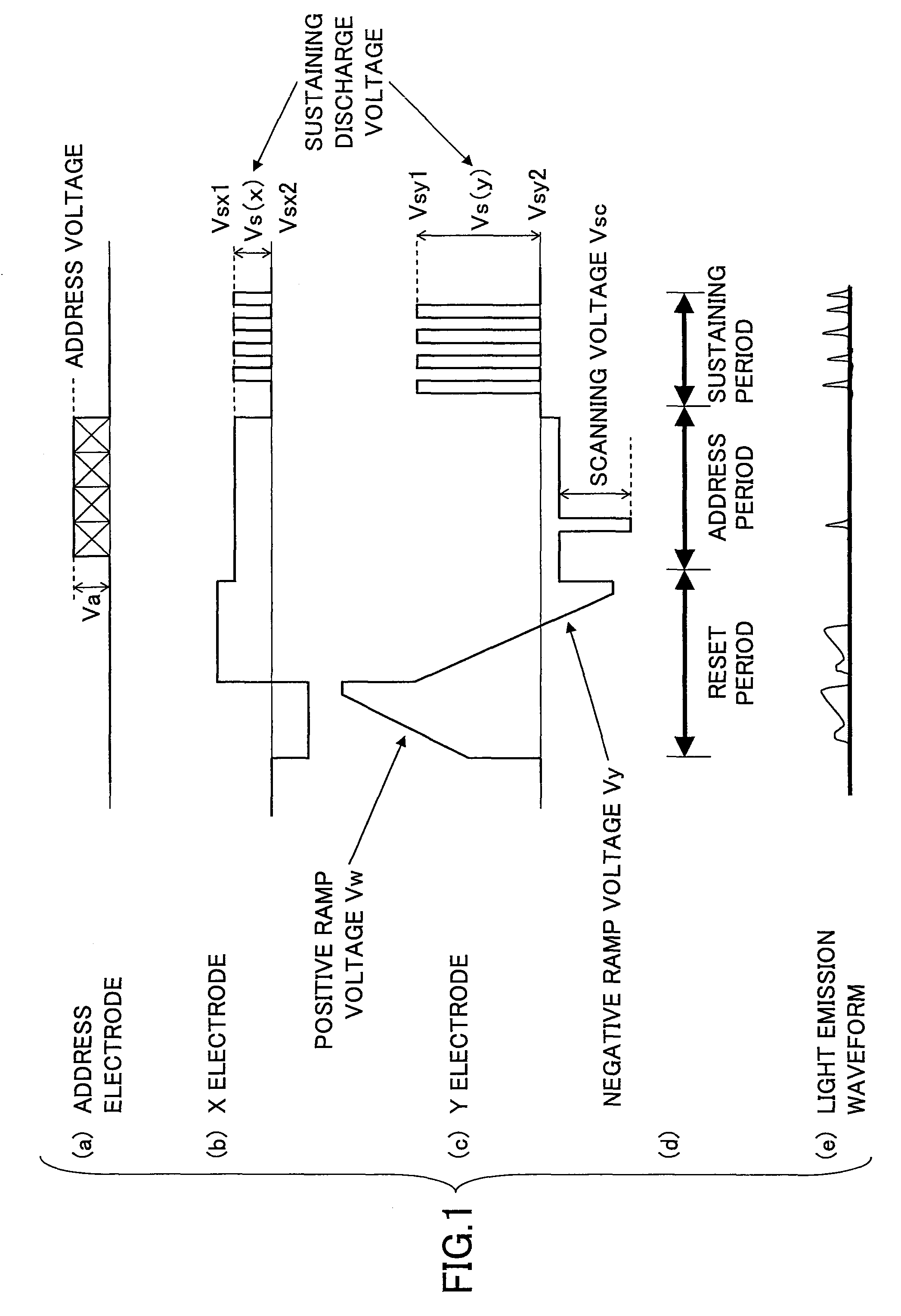
[0074]FIG. 6 is a drawing illustrating examples of driving waveforms applied to the display electrodes (the X electrode 31X and the Y electrode 31Y) and operation timings of the switches SW1x through SW4x and SW1y through SW4y in a plasma display and a plasma display panel driving method according to a third embodiment of the present invention. Similar to FIG. 4 of the first embodiment, FIG. 6 (a) shows a driving voltage waveform of the X electrode 31X and FIG. 6 (b) shows a driving voltage waveform of the Y electrode 31Y. FIG. 6 (c) shows a potential difference obtained by subtracting an electric potential of the Y electrode 31Y from an electric potential of the X electrode 31X. FIG. 6 (d) shows a light emission waveform of the display cell 33. FIG. 6 (e) shows operation timings of the switches SW1x through SW4x of the X sustaining circuit 11X, 12X. FIG. 6 (f) shows operation timings of the switches SW1y through SW4y of the Y sustaining circuit 11Y, 12Y.
[0075]In the second embodime...
PUM
 Abstract
Description
Claims
Application Information
 - R&D
- Intellectual Property
- Life Sciences
- Materials
- Tech Scout
- Unparalleled Data Quality
- Higher Quality Content
- 60% Fewer Hallucinations
Browse by: Latest US Patents, China's latest patents, Technical Efficacy Thesaurus, Application Domain, Technology Topic, Popular Technical Reports.
© 2025 PatSnap. All rights reserved.Legal|Privacy policy|Modern Slavery Act Transparency Statement|Sitemap|About US| Contact US: help@patsnap.com


