
Method for forming silicon trench

a technology of silicon trenches and ladi, applied in the field of silicon trenches, can solve the problems of limited ladi line width and depth, and high cost, and achieve the effect of low cos

Active Publication Date: 2012-06-05
NAT TAIWAN UNIV
View PDF7 Cites 18 Cited by
  • Summary
  • Abstract
  • Description
  • Claims
  • Application Information

AI Technical Summary

Benefits of technology

[0009]An object of the present invention is to provide a low cost method for fabricating highly anisotropic silicon trenches with depth reaching to micrometers scale, and the silicon trenches can be produced in a large-area manner.

Problems solved by technology

However, these methods have several drawbacks.
RIE is a typical method for creating highly anisotropic structures in conventional semiconductor fabrication, but it utilizes expensive instruments and is rarely performed on an ultra-large scale.
KOH wet chemical etching is a low cost and large-area fabrication method, but the etching direction is restricted due to the crystal orientation.
LADI is a rapid etching-free technique for patterning nanostructures in silicon; however, the produced line widths and depths by LADI are limited to sub-micrometers.

Method used


Image

  • Method for forming silicon trench
  • Method for forming silicon trench
  • Method for forming silicon trench

Examples


example

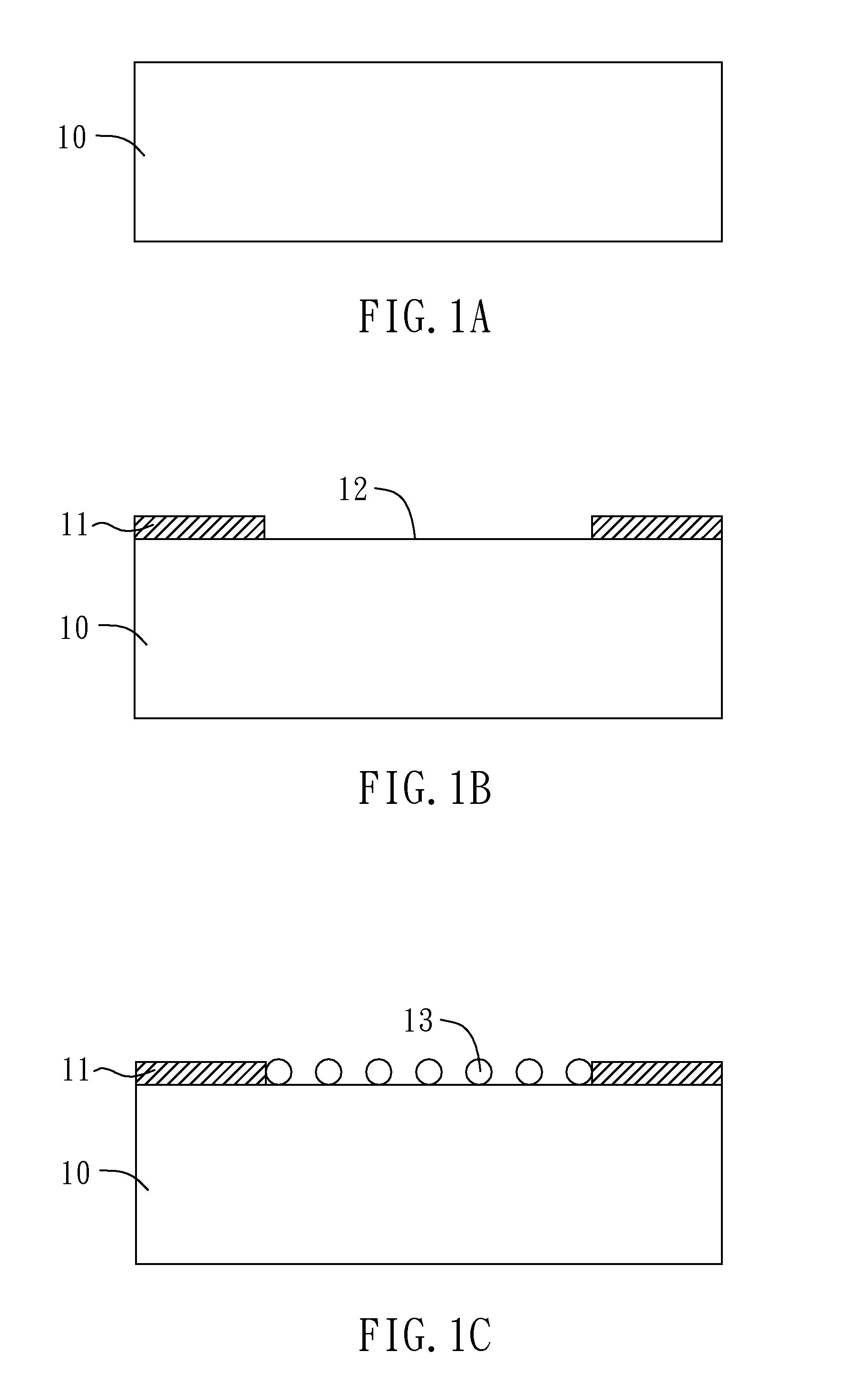
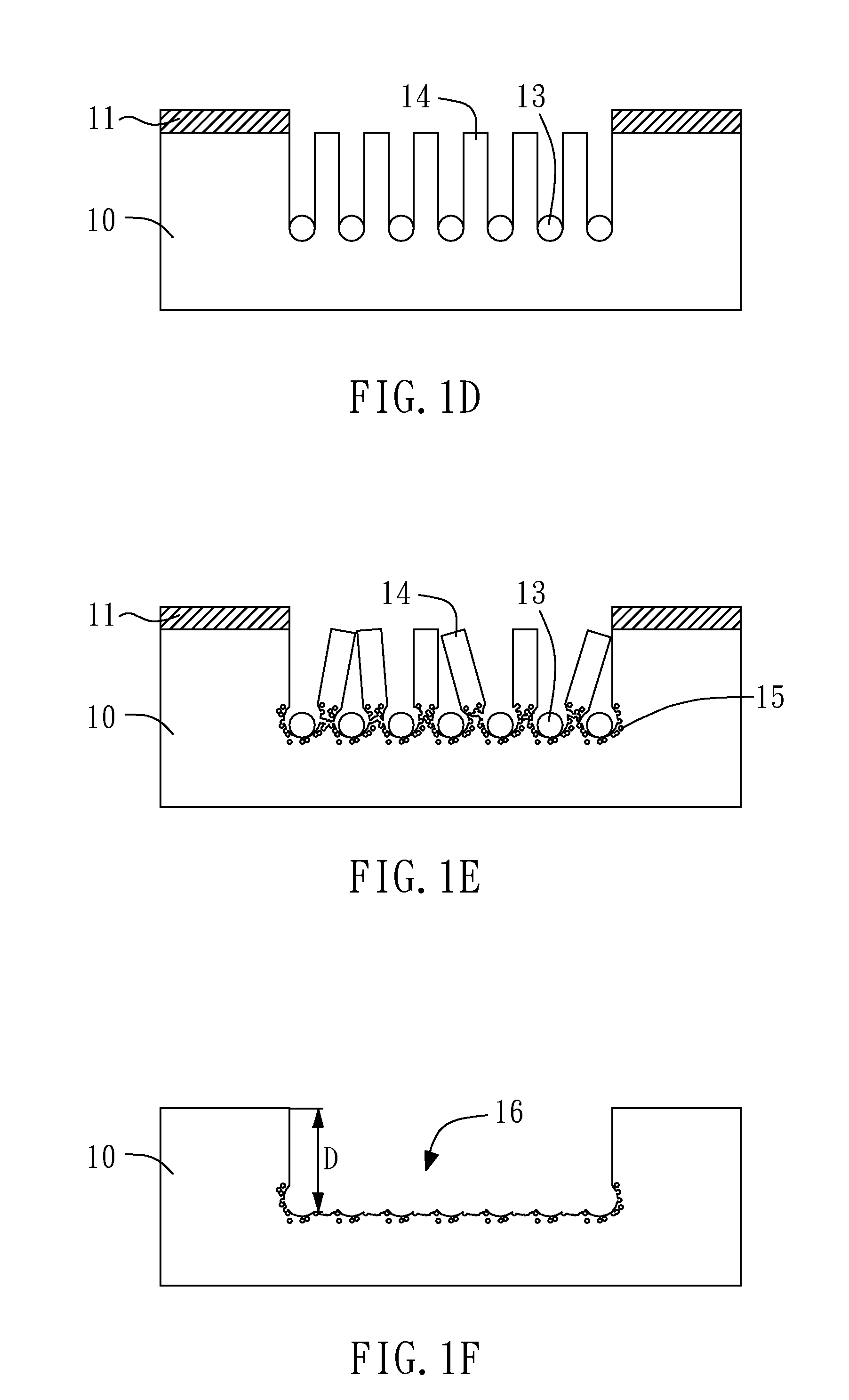
[0027]This example employs silver as the center of the redox reaction, illustrating how silicon trenches are formed. First, a p-type Si wafer with a resistance of 1-10 Ωcm is provided and cleaned. Then, the Si wafer is spin coated with a photoresist (positive photoresist S1813) and the photoresist is patterned to define etching areas by using a typical photolithography process. Then, the Ag catalysts were subsequently deposited on the etching areas through EMD method. For example, the Si wafer is immersed in an aqueous HF / AgNO3 solution including 0.02 mol / L AgNO3 and 10 vol. % HF in deionized water about 20 sec, so as to deposit Ag catalysts on the etching areas.

[0028]Then, the silicon wafer is immersed in the above HF / AgNO3 solution again for 10 to 30 min. Alternatively, the silicon wafer is immersed in an aqueous HF / H2O2 solution including 0.6 vol. % H2O2 and 10 vol. % HF in deionized water for about 10 to 30 min. The Ag ions of the solution will be selectively deposited on the Ag...


PUM

PropertyMeasurementUnit
temperatureaaaaaaaaaa
depthaaaaaaaaaa

Abstract

A method for forming a silicon trench, comprises the steps of: defining an etching area at a silicon substrate; forming metal catalysts at the surface of the etching area; immersing the silicon substrate in a first etching solution thereby forming anisotropic silicon nanostructures in the etching area; immersing the silicon substrate in a second etching solution thereby resulting in the silicon nanostructures being side-etched and detached from the silicon substrate, thus forming the silicon trench.

Description

CROSS-REFERENCE TO RELATED APPLICATIONS[0001]This application is a continuation-in-part of co-pending U.S. application Ser. No. 12 / 790,331, filed May 28, 2010 and entitled SILICON NANOSTRUCTURES AND METHOD FOR PRODUCING THE SAME AND APPLICATION THEREOF, and claims the priority of Taiwan Patent Application No. 099134859, filed on Oct. 13, 2010, the entire contents both of which are incorporated herein by reference.BACKGROUND OF THE INVENTION[0002]1. Field of the Invention[0003]The present invention relates to methods for forming semiconductor trenches, particularly silicon trenches.[0004]2. Description of Related Art[0005]Highly anisotropic etching structures in silicon have many applications. For example, anisotropic trenches are required during the fabrication of semiconductor devices, such as optical biosensors, optical switches, and metal-oxide-semiconductor field effect transistor devices.[0006]The dimensions of these trenches typically range from 1-4 μm in width and 0.5-5 μm in...

Claims


Application Information

Patent Timeline
Patent Type & Authority Patents(United States)
IPC IPC(8): H01L21/311
CPCH01L31/022425H01L31/1804H01L21/30608B82Y10/00H01L29/0665Y10S977/888Y10S977/856Y02E10/547Y02P70/50
Inventor LIN, CHING-FUHHUNG, SHIH-CHESYU, SHU-JIA
Owner NAT TAIWAN UNIV
Learn More