Display device and production method thereof

a technology of a display device and a production method, applied in the field of display devices, can solve the problems of increasing the loss of materials, difficult to simplify the process, and limited pattern shape, and achieve the effect of uniform thickness distribution and without reducing productivity

Inactive Publication Date: 2012-03-27
SHARP KK
View PDF25 Cites 2 Cited by
  • Summary
  • Abstract
  • Description
  • Claims
  • Application Information

AI Technical Summary

Benefits of technology

[0038]According to the first or second display device of the present invention, the active matrix substrate has a pixel division configuration. Therefore, the phenomenon in which gradation dependency of display luminance is different between when the display is viewed in the front direction and when the display is viewed in an oblique direction is resolved. In addition, despite the pixel division configuration, the CF substrate can be produced by an ink-jet method without reducing the productivity, and high-quality colored layers having a uniform thickness distribution can be formed.

Problems solved by technology

Therefore, the processes are difficult to simplify.
In addition, spin coating in the application step increases loss of materials.
According to the electrodeposition method, the pattern shape is limited.
Further, a high-definition pattern is difficult to form by the printing method.
If the CF substrate is prepared by an ink-jet method, inks might be mixed between adjacent pixels to cause a color mixing defect.
If a pixel division configuration that has been recently adopted to a liquid crystal TV and the like as a wide viewing angle technology is employed in combination with the method of producing a CF substrate by an ink-jet method, the bank structure might hinder drawing of a colored layer pattern that is formed with an ink-jet apparatus.
Even if droplets in a required amount are injected, the ink is difficult to spread into the vicinity a hem of the TFT shielding part 30, and the ink is not uniformly spread.
Therefore, it takes a long time to complete the ink injection, which leads to a reduction in production efficiency of the colored layers.

Method used


Image

  • Display device and production method thereof
  • Display device and production method thereof
  • Display device and production method thereof

Examples


embodiment 1

“Embodiment 1”

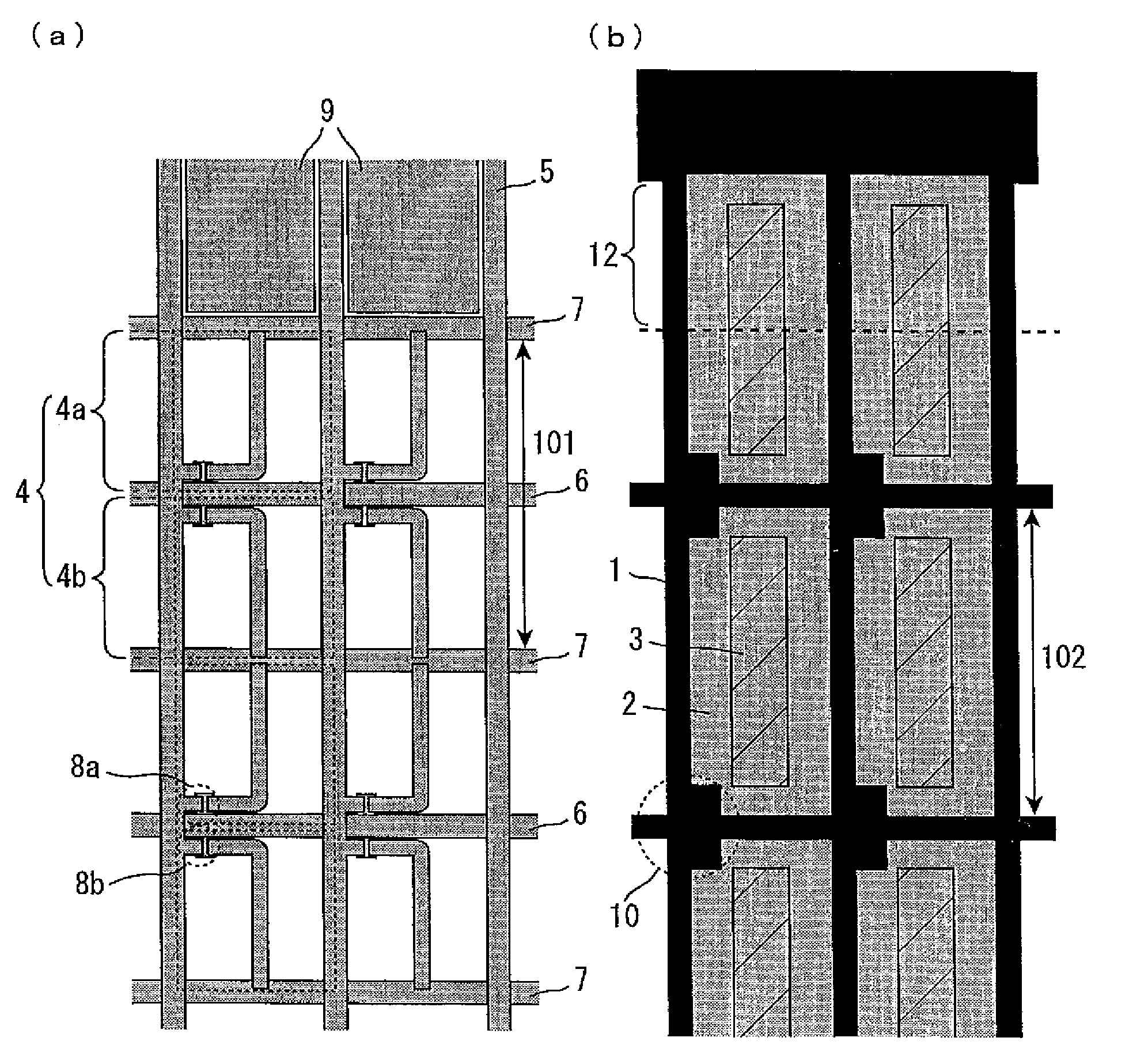
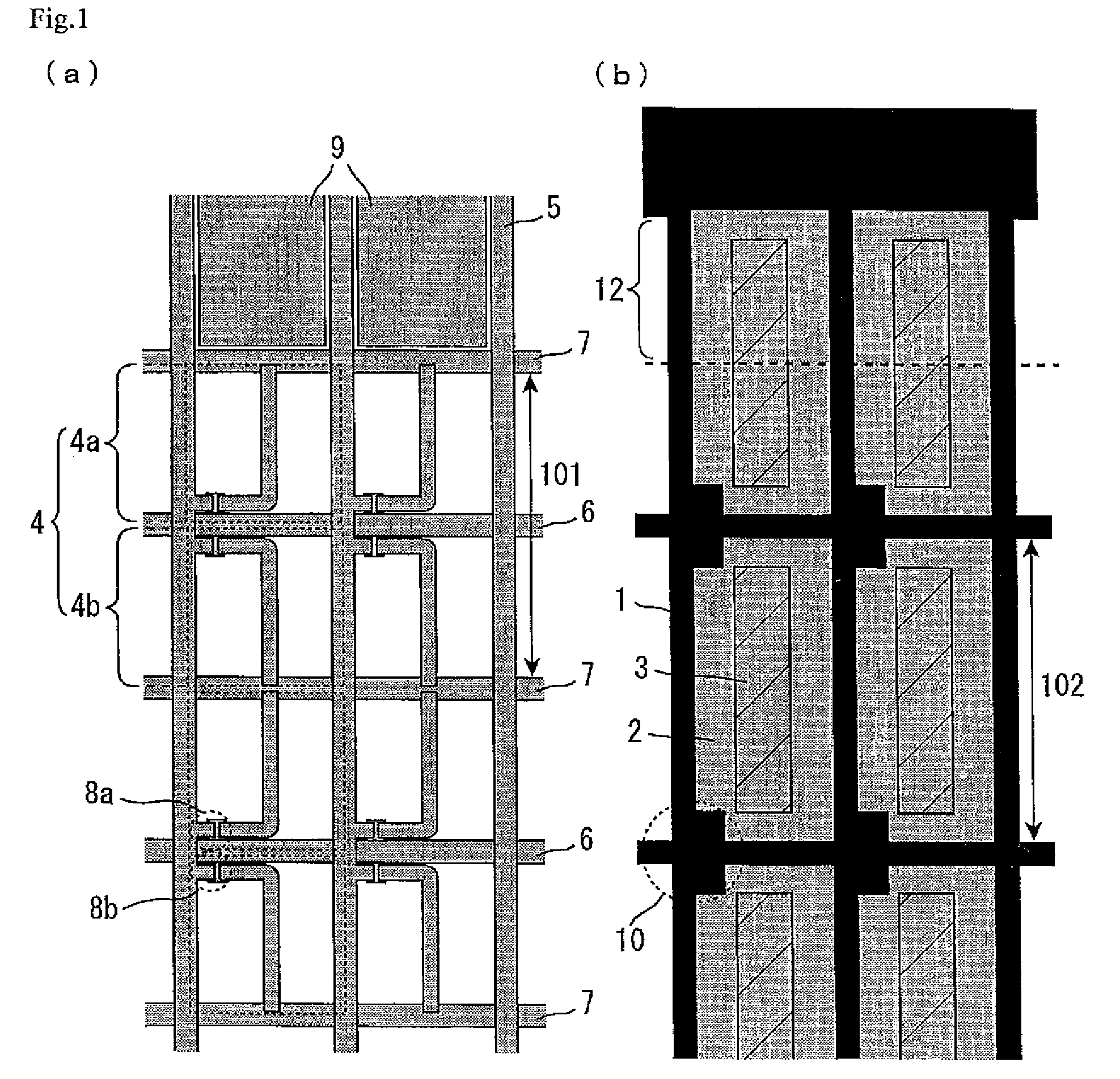
[0043]A display device in accordance with Embodiment 1 includes a TFT substrate (active matrix substrate) and a CF substrate facing each other. FIG. 1 is a planar view schematically showing each substrate in the display device in accordance with Embodiment 1. FIG. 1(a) shows the TFT substrate. FIG. 1(b) shows the CF substrate. The display device in Embodiment 1 further includes components which a common liquid crystal display has, as well as the TFT substrate and the CF substrate. For example, a liquid crystal layer is arranged between the TFT substrate and the CF substrate facing each other. On the sides opposite to the liquid crystal layer of the both substrates, a polarizer and various optical films and the like are arranged. A backlight is also arranged if the display device is a transmissive or transflective liquid crystal display device.

[0044]As shown in FIG. 1(a), a plurality of signal lines 5 and a plurality of scanning lines 6 are arranged on the TFT substrate...

embodiment 2

“Embodiment 2”

[0053]A display device in accordance with Embodiment 2 is the same as in Embodiment 1, except that the dummy colored layer 9a and the dummy metal pattern 12 in the display device in Embodiment 1 are not arranged and that the CF substrate does not include the bank in the part overlapping with the scanning line positioned at the end of the display region. FIG. 2 is a planar view schematically showing a CF substrate of the display device in accordance with Embodiment 2. According to Embodiment 2, as measures against the difference between the pixel formation period 101 in the TFT substrate and the colored layer formation period 102 in the CF substrate, the bank is not formed in the part overlapping with the scanning line positioned at the end of the display region. As a result, a colored layer 22 positioned at the end of the display region is formed to have an area 1.5 times larger than that of another colored layer. That is, the colored layers 22 in Embodiment 2 include ...


PUM

PropertyMeasurementUnit
distanceaaaaaaaaaa
areaaaaaaaaaaa
luminanceaaaaaaaaaa

Abstract

A display device includes an active matrix substrate and a color filter substrate facing each other, wherein the active matrix substrate includes a scanning line, a signal line, and a switching element, and has a pixel, the switching element being arranged at an intersection of the scanning line and the signal line, the pixel including two sub-pixels, the two sub-pixels being arranged with the scanning line or the signal line therebetween, the color filter substrate includes a bank and a plurality of colored layers surrounded by the bank, the bank being arranged in regions overlapping with the signal line, and the switching element, and the plurality of colored layers include the first colored layer and the second colored layer, the first colored layer overlapping with one sub-pixel positioned at an end and a region outside a sub-pixel-arranged region, and the second colored layer overlapping with two sub-pixels.

Description

BACKGROUND OF THE INVENTION[0001]1 Field of the Invention[0002]The present invention relates to a display device and a production method thereof. More specifically, the present invention relates to a display device such as a liquid crystal display device, which provides color display using colored layers formed by a method of applying a droplet, such as an inkjet method, and to a production method of such a display device.[0003]2 Description of the Related Art[0004]In display devices such as a liquid crystal display device, various contrivances have been introduced to prevent a reduction in contrast ratio, a change in color tone, darkening of display gradation, and the like when a screen is viewed in an oblique direction. Further, the following problem has been recently pointed out. A difference in gradation level of display luminance between when the screen is viewed in the front direction and when it is viewed in an oblique direction causes a difference in display state depending ...

Claims


Application Information

Patent Timeline
Patent Type & Authority Patents(United States)
IPC IPC(8): G02F1/1335
CPCG02F1/133516G02B5/201G02B5/223G02F1/133512G02F1/136213G02F1/13624G02F2201/52
Inventor NIIYA, HIROTAKA
Owner SHARP KK
Why Eureka
Try Eureka