Driving circuit including shift register and flat panel display device using the same
a technology of shift register and display device, which is applied in the direction of static storage, digital storage, instruments, etc., can solve the problems of large volume, heavy weight, and drawbacks of crts
- Summary
- Abstract
- Description
- Claims
- Application Information
AI Technical Summary
Benefits of technology
Problems solved by technology
Method used
Image
Examples
first embodiment
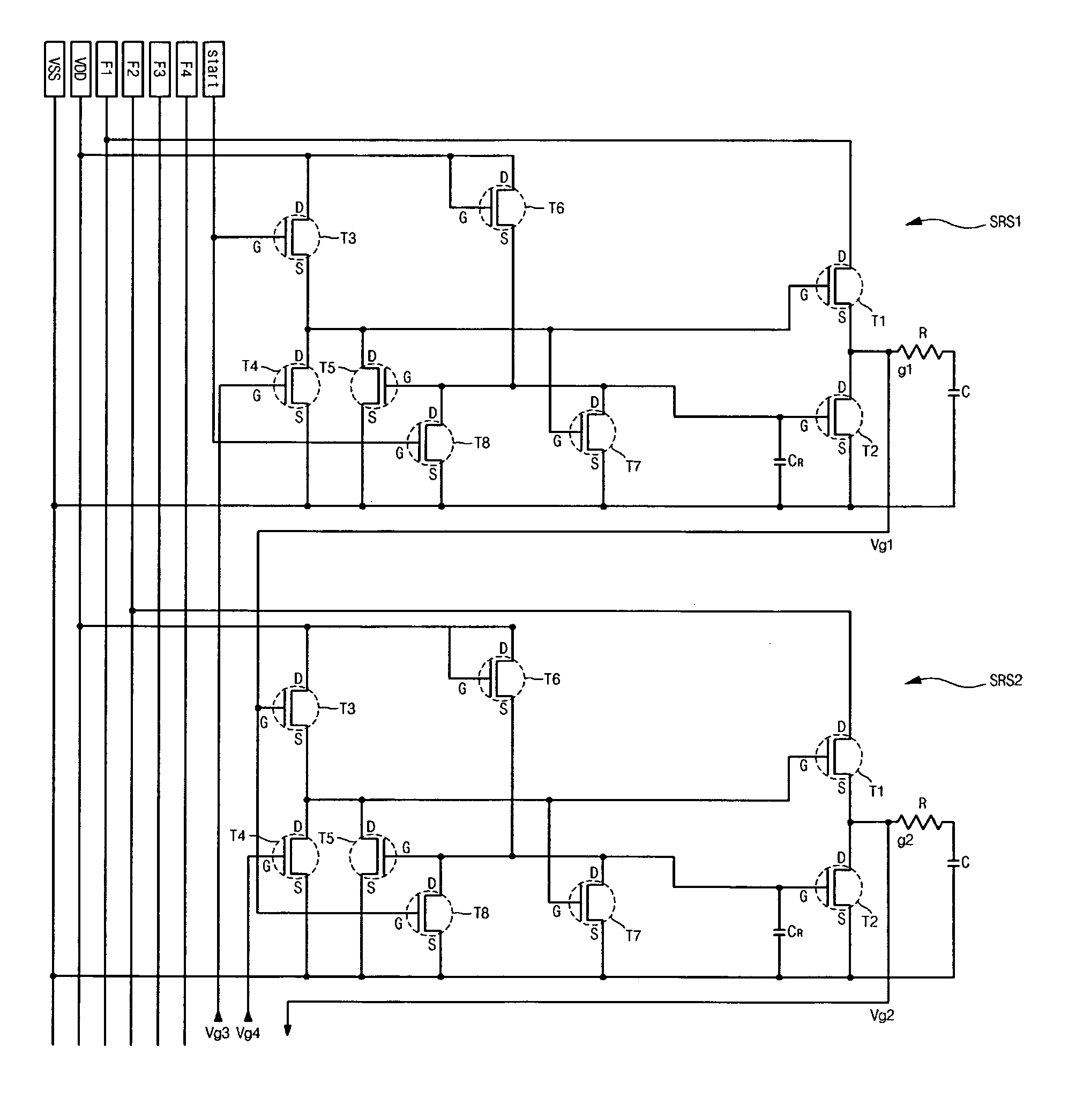
[0060]FIG. 9 is a schematic circuit diagram illustrating a driving circuit in a display panel for a flat panel display device according to the present invention.
[0061]As illustrated in FIG. 9, the driving circuit includes a plurality of shift register stages “SRS1,”“SRS2”, “SRS3” and “SRS4”. For the sake of brevity, only four shift register stages are shown and explained. Each of the shift register stages “SRS1,”“SRS2”, “SRS3” and “SRS4” includes a shift register unit “SRU1,”“SRU2”, “SRU3” or “SRU4”, a first transistor “T1” and a second transistor “T2”, and a first AND operator “A1” and a second AND operator “A2”. An RS flip-flop circuit is used for the shift register units “SRU1,”“SRU2”, “SRU3” and “SRU4”, and an AND gate circuit is used for the first and second operators “A1” and “A2”. Each of the shift register stages “SRS 1,”“SRS2”, “SRS3” and “SRS4” is connected to the corresponding gate line “g1”, “g2”, “g3” or “g4”. An array resistor R and an array capacitor C connected to ea...
second embodiment
[0106]FIGS. 21 to 23 are schematic timing charts showing three examples of signals input to and output from the driving circuit of FIG. 20 according to the present invention.
[0107]As shown in FIGS. 21 to 23, three-phase form generation clocks “F1” to “F3” have wave shapes “WS1” to “WS3” corresponding to the four-phase form generation clocks of FIGS. 10 to 12, respectively, except for a period of the form generation clock. In other words, because the three-phase form generation clocks “F1” to “F3” are input to the corresponding shift register stages, the period “T2” of the three-phase form generation clocks “F1” to “F3” is less than the period “T1” of the four-phase form generation clocks. In these examples, the period “T2” is equal to ¾“T1”. The output signals of the driving circuit can have a variety of shapes even after the driving circuit is formed by providing clock signals having a variety of shapes to the driving circuit. Accordingly, a fixation problem of output signal shape ...
PUM
 Abstract
Description
Claims
Application Information
 - R&D
- Intellectual Property
- Life Sciences
- Materials
- Tech Scout
- Unparalleled Data Quality
- Higher Quality Content
- 60% Fewer Hallucinations
Browse by: Latest US Patents, China's latest patents, Technical Efficacy Thesaurus, Application Domain, Technology Topic, Popular Technical Reports.
© 2025 PatSnap. All rights reserved.Legal|Privacy policy|Modern Slavery Act Transparency Statement|Sitemap|About US| Contact US: help@patsnap.com


